- Mark as New
- Bookmark
- Subscribe
- Mute
- Subscribe to RSS Feed
- Permalink
- Report Inappropriate Content
Hello,
I have refered the AN754:MIPI D-PHY Solution with Passive Resistor Networks in Intel® Low-Cost FPGAs to acheive mipi transmission on Cyclone IV. We can see in the solution handlebook that, The single-ended
mode uses LVCMOS or HSTL I/O standard for low-power mode, and differential I/O standard (LVDS) for high-speed mode. And we can also see that in high speed mode, the Tx IO standard is Differential HSTL-18, and the hardware design is like the following figure:
but when I do my pin planner, I find the high speed pins I selected do not support the Differential HSTL-18(will get a error report when compile), only support 1.8-V HSTL CLASS I or II(compile successfully). I want to know if the high-speed pins must use differential 1.8-V HSTL IO standard? The hardware design as shown below. I will be grateful if there is someone can give me a reply.Thanks for much.
Link Copied
- Mark as New
- Bookmark
- Subscribe
- Mute
- Subscribe to RSS Feed
- Permalink
- Report Inappropriate Content
JChen562,
Can you provide me the details of your design for further debug?
May I know your Cyclone IV specific OPN? And which I/O bank do you assigned Differential HSTL-18?
Anyway, can you re-send your hardware design? I cant see you diagram above.
Thanks
- Mark as New
- Bookmark
- Subscribe
- Mute
- Subscribe to RSS Feed
- Permalink
- Report Inappropriate Content
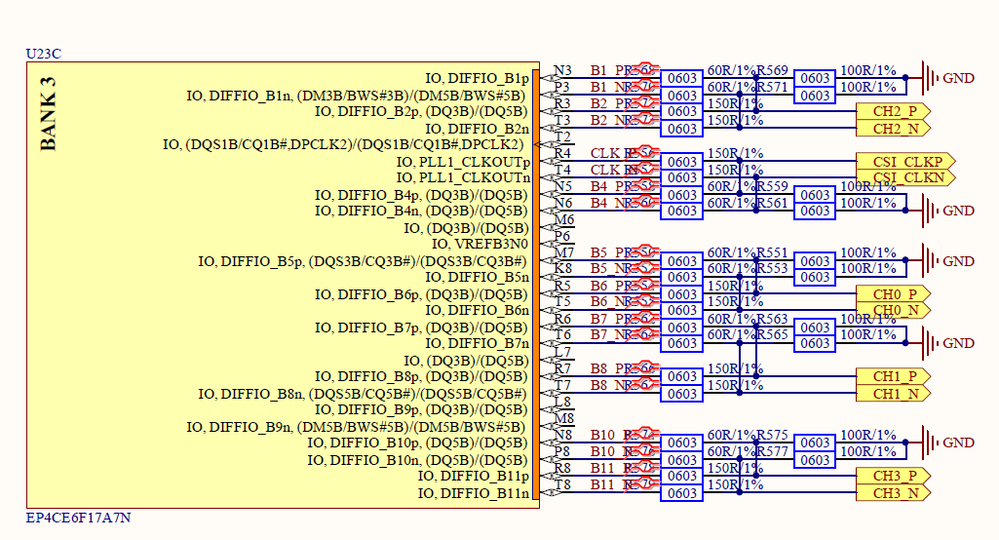
Thanks for your answer. the specific OPN is EP4CE6F17. And can you see the hardware design this time? I use bank3 for mipi design(R4 & T4 as differential pair for HS clk, N5 & N6 as single end for LP clk, R5 & T5 for HS data lane0, M7 & K8 as single end for LP data lane0, R7 & T7 for HS data lane1, R6 & T6 for LP data lane1, R3 & T3 for HS data lane2, N3 & P3 for LP data lane2, R8 & T8 for HS data lane3, N8 & P8 for LP data lane3, as shown in the image below). in my opinions, these pins need to design as inout type to do state switch between HS and LP. And there are two questions when I design my qurtus project.
- R4 & T4 do not support bidirection(only output) when I choose differential 1.8-V HSTL IO standard in my pin planner, so I have to choose 1.8-V HSTL CLASS I IO standard.
- all HS data lanes I list above do not have differential 1.8-V HSTL IO standard in the pin planner, so I have to choose 1.8-V HSTL CLASS I IO standard.
It compiled successfully, but I think it is not satisfied with the requirement in AN754. Could you give me some suggestions about my questions? Is there something wrong in my understanding?
- Mark as New
- Bookmark
- Subscribe
- Mute
- Subscribe to RSS Feed
- Permalink
- Report Inappropriate Content
Hi,
sorry to reopen this old thread.
Are there any news regarding the open questions?
Thank you
- Subscribe to RSS Feed
- Mark Topic as New
- Mark Topic as Read
- Float this Topic for Current User
- Bookmark
- Subscribe
- Printer Friendly Page
