Scott Bair is a key voice at Intel Labs, sharing insights into innovative research for inventing tomorrow’s technology.
Highlights:
- The world's premier conference devoted to integrated circuits development, IEEE Custom Integrated Circuits Conference (CICC) 2023 will run from April 23 to 26 in San Antonio, Texas.
- Intel Labs is excited to be nominated for the Best Regular Paper Award for its innovative research ‘A 3D-integrated 8λ x 32 Gbps/λ Silicon Photonic Microring-based DWDM Transmitter’ at this year’s conference.
- Compared to prior work, the transmitter demonstrates 28% higher bandwidth and integrates all the necessary photonics and electronics required for co-packaging with bandwidth-intensive compute silicon.
The world's premier conference devoted to integrated circuits development, IEEE Custom Integrated Circuits Conference (CICC) 2023, will run from April 23 to 26 in San Antonio, Texas. The conference program is a blend of oral presentations, exhibits, panels and forums in which researchers present original first published technical work and innovative circuit techniques that tackle practical problems. Intel Labs researchers present ‘A 3D-integrated 8λ x 32 Gbps/λ Silicon Photonic Microring-based DWDM Transmitter’ detailing our latest contribution to silicon photonics, and the transmitter’s achievement over prior works.
“We are excited to present our innovative research at this year’s conference and honored to be nominated for CICC’s Best Regular Paper Award.”
- James Jaussi, Senior Principal Engineer and director of the PHY Research Lab at Intel Labs.
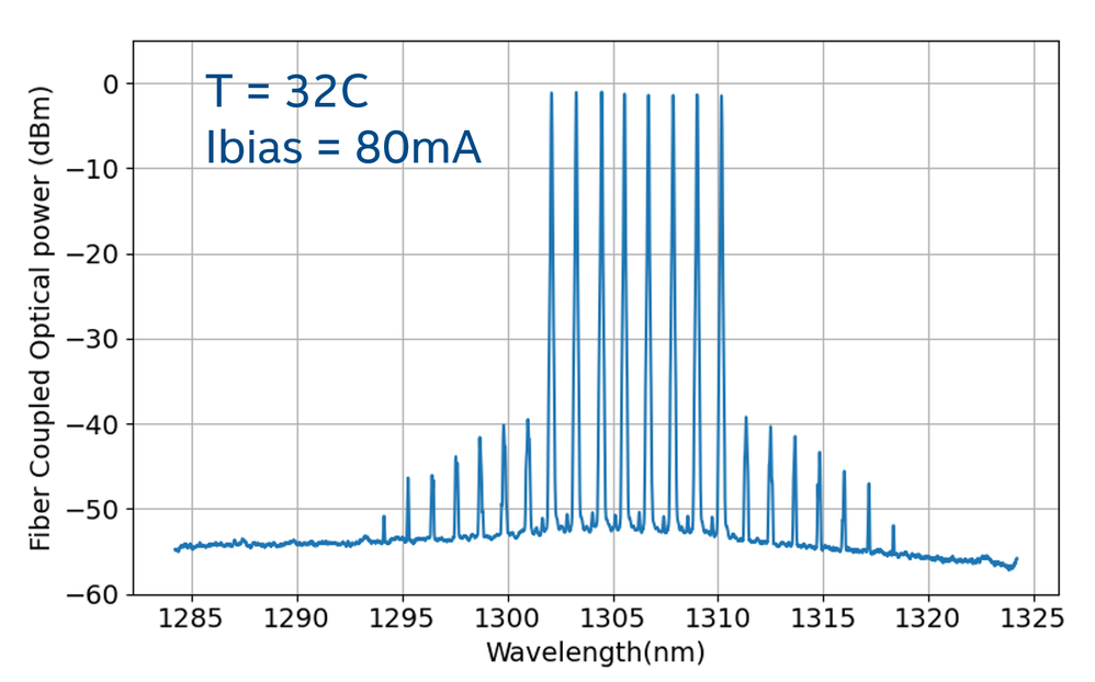
In June 2022, Intel Labs announced a significant advancement in its integrated photonics research to increase communication bandwidth between compute silicon in data centers and across networks. The research featured innovations in multiwavelength integrated optics, including the demonstration of an eight-wavelength distributed feedback (DFB) laser array that is fully integrated on a silicon wafer and delivers excellent output power uniformity of +/- 0.25 decibel (dB) and wavelength spacing uniformity of ±6.5% that exceed industry specifications.
Figure 1. (a) The illustration shows an eight-channel hybrid III-V/silicon distributed feedback laser array. (b) DFB array measured spectrum.
Intel is committed to developing solutions to meet the growing demand for a more efficient and resourceful network infrastructure. As part of this ongoing pursuit, Intel Labs has continued to support research in this area. Our current work details a novel silicon photonic microring-based dense wavelength division multiplexing (DWDM) transmitter that includes the laser announced in 2022 as the light source.
Silicon photonics-based optical I/O is a promising technology direction to meet the ever growing off-chip I/O bandwidth needs of data-intensive computing. While silicon photonic (SiPh) transceivers are increasingly being used in pluggable modules for data center communications, the power efficiency and latency constraints for their integration in XPU/switch packages are more stringent, requiring different solutions. Ring resonator-based transceiver architectures are attractive for this application due to their small footprint and suitability for DWDM, which enables energy-efficient bandwidth scaling.
Recent system demonstrations of ring-based transceivers have shown per-wavelength data rates of up to 16 Gb/s and low bit error rates (<1e-12); however, these require an external multi-wavelength laser source, increasing optical path loss and requiring additional fibers be attached to the compute package. Prior demonstrations have shown higher baud rates in ring-based systems, but modulate only one or two wavelengths at a time. This paper presents a SiPh microring-based transmitter that includes all photonic and electronic components needed to support simultaneous modulation of eight 200 GHz-spaced wavelengths at 32 Gbps/λ for an aggregate bandwidth of 256 Gbps/fiber.
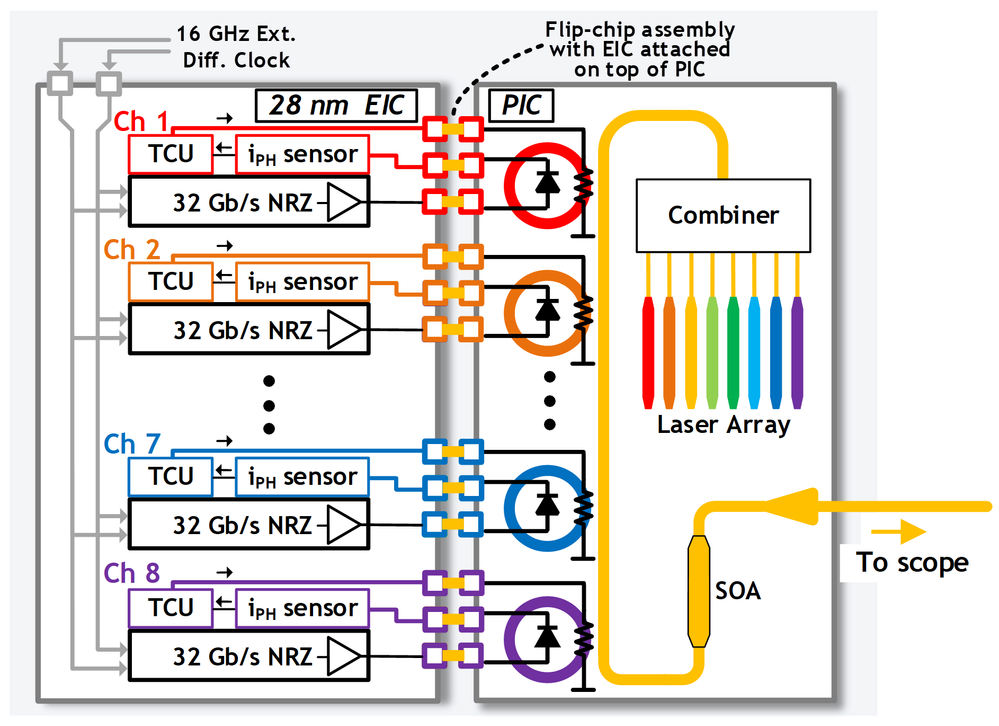
The optical transmitter consists of a flip-chip integrated silicon photonic integrated circuit (PIC) and an electronic IC (EIC), as shown in Figure 2 below. The PIC includes a multi-wavelength source composed of a distributed feedback (DFB) laser array followed by a combiner which generates 8 wavelengths centered at 1310 nm with 200 GHz spacing. The modulator bank consists of 8 cascaded microring modulators (MRMs) , each with s an integrated heater to align its resonance with the target laser wavelength. A thermal control unit (TCU) in the EIC senses the MRM photocurrent and modulates the MRM heater power to achieve the desired insertion loss (IL), stabilizing the lock point against process and temperature variation. The EIC also integrates a clock receiver, pattern generator, and high-swing MRM drivers. A semiconductor optical amplifier following the modulator bank amplifies the transmitter output before coupling it externally.
Figure 2. Hybrid integrated Optical Transmitter (OTX) showing EIC and PIC details.
The transmitter achieves better than 4.9 dB ER across all 8 channels with <1 dB difference in optical modulation amplitude. Compared to prior work, this transmitter demonstrates 28% higher bandwidth and integrates all the necessary photonics and electronics required for co-packaging with bandwidth-intensive ASICs. Measured per-channel power dissipation of the transmitter electronics (excluding microring modulator heater power) is 43 mW at 32 Gbps, yielding 1.35 pJ/bit efficiency.
Intel is committed to paving the way for a more efficient and resourceful network infrastructure, and as such, our efforts in silicon photonics research are ongoing. We hope to further advance the performance of essential silicon photonic building blocks for light generation, amplification, modulation, and detection, while integrating them with energy-efficient CMOS interface circuits through advanced packaging technologies.
 Scott Bair is a Senior Technical Creative Director for Intel Labs, chartered with growing awareness for Intel’s leading-edge research activities, like AI, Neuromorphic Computing and Quantum Computing. Scott is responsible for driving marketing strategy, messaging, and asset creation for Intel Labs and its joint-research activities. In addition to his work at Intel, he has a passion for audio technology and is an active father of 5 children.
Scott has over 23 years of experience in the computing industry bringing new products and technology to market. During his 15 years at Intel, he has worked in a variety of roles from R&D, architecture, strategic planning, product marketing, and technology evangelism. Scott has an undergraduate degree in Electrical and Computer Engineering and a Masters of Business Administration from Brigham Young University.
You must be a registered user to add a comment. If you've already registered, sign in. Otherwise, register and sign in.


