- Mark as New
- Bookmark
- Subscribe
- Mute
- Subscribe to RSS Feed
- Permalink
- Report Inappropriate Content
hello ,
[ Scenario] We can run AN829 PCIE driver on Arria10 EVM Board.
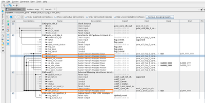
In the FPGA design example, [pcie_a10_hip] -> [rxm_bar2] can read/write to [ FPGA Emif -> ctrl_amm Slave Node] where we have 2GB DDR4 on fpga side (0x0 ~ 0x40000000).
Linux Host can acess (read & write) the FPGA DDR4 through PCIE_BAR2, as following :
iowrite32 (cpu_to_le32(data), (u32 *)(bk_ptr->bar[BAR2]+byte_offset));
My question: on my test, that PCIE_BAR2 can only maps "512MBytes" totally address space, which is mapped to FPGA-DDR4 "from 0x0 to 0x10000000" (the top 512MB). If I need access to the FPGA-DDR4 1GB starting address 0x20000000 ~ 0x30000000, how can I realize this ? Where to configure PCIE parameter to make BAR2 maps to this [0x2000 0000 ~ 0x3000 0000] ddr memory space ? any ideas ?
Thanks in advance
- Mark as New
- Bookmark
- Subscribe
- Mute
- Subscribe to RSS Feed
- Permalink
- Report Inappropriate Content
I forgot to explain further. In AN829, DDR4 is connected to PCIe DMA port which means DDR4 can only be accessed via DMA control only.
That's why I suggested you to switch to use PCIe IP without enabling the DMA logic insides the IP. Then user can connect PCIe IP directly to memory (like DDR4) and access it.
Thanks.
Regards,
dlim
Link Copied
- Mark as New
- Bookmark
- Subscribe
- Mute
- Subscribe to RSS Feed
- Permalink
- Report Inappropriate Content
HI,
Platform designer only specify offset address, EMIF IP, on chip memory and PCIe IP setting.
Moving data between CPU host memory to FPGA DDR4 memory or on chip memory is controlled by DMA descriptor controller.
- Meaning DMA driver software is the one responsible to configure DMA descriptor to tell it to access which memory address location.
I am not familiar with driver software design but you can try hack DMA driver design DDR4 address offset parameter to see if it helps to change the DMA memory access address to none default 0 address
- Look for altera_dma.h in "AN829_driver" folder
- goto either Arria 10 or Cyclone 10 section (depend on which FPGA product you are using), search for OFFCHIP_MEM_BASE parameter and change it to some other offset value
- Just make sure the new offset value doesn't overwrite with on chip memory address space (ONCHIP_MEM_BASE)
If it still failed, then you will need to study on how to write up DMA driver...
Thanks.
Regards,
dlim
- Mark as New
- Bookmark
- Subscribe
- Mute
- Subscribe to RSS Feed
- Permalink
- Report Inappropriate Content
- Mark as New
- Bookmark
- Subscribe
- Mute
- Subscribe to RSS Feed
- Permalink
- Report Inappropriate Content
HI,
It doesn't work like that. You are looking at example design that use (PCIe + DMA) IP.
If you just want to use PCIe IP that interact with memory directly, then pls consider to check out below example design that use (PCIe) only, no DMA
- https://www.intel.com/content/dam/www/programmable/us/en/pdfs/literature/ug/ug-dex-a10-pcie-avmm.pdf
- This is the example design that you can generate from PCIe IP directly
- This example design currently connect to on chip RAM but you can replaced with DDR4 if you want
Thanks.
Regards,
dlim
- Mark as New
- Bookmark
- Subscribe
- Mute
- Subscribe to RSS Feed
- Permalink
- Report Inappropriate Content
I forgot to explain further. In AN829, DDR4 is connected to PCIe DMA port which means DDR4 can only be accessed via DMA control only.
That's why I suggested you to switch to use PCIe IP without enabling the DMA logic insides the IP. Then user can connect PCIe IP directly to memory (like DDR4) and access it.
Thanks.
Regards,
dlim
- Mark as New
- Bookmark
- Subscribe
- Mute
- Subscribe to RSS Feed
- Permalink
- Report Inappropriate Content
- Mark as New
- Bookmark
- Subscribe
- Mute
- Subscribe to RSS Feed
- Permalink
- Report Inappropriate Content
You are welcome !
- Subscribe to RSS Feed
- Mark Topic as New
- Mark Topic as Read
- Float this Topic for Current User
- Bookmark
- Subscribe
- Printer Friendly Page
