- Mark as New
- Bookmark
- Subscribe
- Mute
- Subscribe to RSS Feed
- Permalink
- Report Inappropriate Content
Hi,
I am havin FIFO underflow in my design. It works fine and I see the output (DVI 1080 progressive input video and output video) on display with the nios ii processor with run time control of the cvi and cvo usign open core i2c bus to program the registers of cvo and cvi in nios II EDS. The design path CVI -> frame buffer -> ddr2 memory->clock crossing brige->-CVO , but as soon as I introduce any vip suite image processing component in the system such as median filter or 2d fir filter I get a FIFO underflow with a flickering or no output. Although ther is no extra slack in any path. The design path CVI -> frame buffer -> color plane sequencer parallel to series -> 2D fir filter -> color plane sequencer series to parallel -> -CVO. frame buffer read and write master -> clock crossing brige-> ddr2 memory. I have debugged the code and I am recieving the DVI input properly. I write a 1 to the sticky bit to clear any previous underflow and set the Go bit in the CVO. There is an underflow as soon as I start the CVO component. I have attached the design in the thread. ----------------------------------------------------------- With 10.1sp1 on Cyclone III development board. CVO and CVI input and output image with DVI 1920 x 1080 format progressive. have all the CVI CVO and other sdc constraints in the design no setup or hold slack . only a removal slack one path ddr2 memory frequency 150 MHz with 64 bit local interface width system clk frequency 100 Mhz dvi clock freq 130 Mhz ----------------------------------------------------------------- Does anyone know why is there an underflow in the CVO? Please Help Thanks Sneha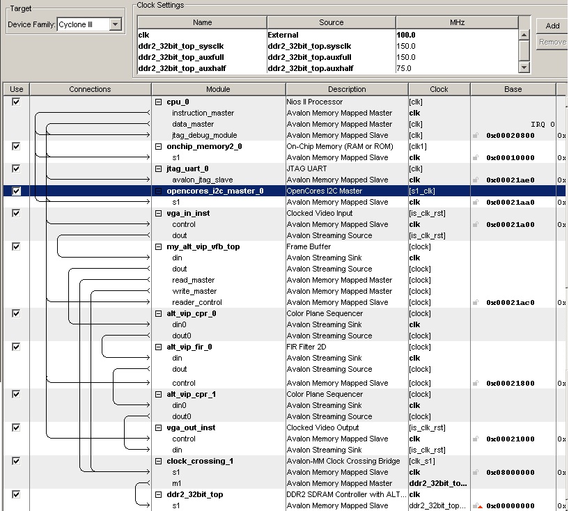
Link Copied
2 Replies
- Mark as New
- Bookmark
- Subscribe
- Mute
- Subscribe to RSS Feed
- Permalink
- Report Inappropriate Content
The time to fill the buffer in the FIR filter may cause some problem. I will put the FIR filter before the Frame Buffer to make sure the CVO has its data when needed.
The Frame Buffer can also turn on the Separate Clock option, so that the Avalon MM output can be connected to the memory without using a clock crossing bridge.- Mark as New
- Bookmark
- Subscribe
- Mute
- Subscribe to RSS Feed
- Permalink
- Report Inappropriate Content
The purpose of adding the clock crossing bridge was to have a buffering mechanism to pipeline multiple read and write transfers. There is an initial latency penalty for first read and write operation but it has a parameterizeable FIFO for slave to master and master to slave signals thus allowing burst transfers across clock domains. It can queue multiple transfers to maintain the system throughput.
I think I have serious bandwidth problem in the design that is what I could make out by reading other posts on the same topic. But dont know how to remove them. Any help ??
Reply
Topic Options
- Subscribe to RSS Feed
- Mark Topic as New
- Mark Topic as Read
- Float this Topic for Current User
- Bookmark
- Subscribe
- Printer Friendly Page