- Mark as New
- Bookmark
- Subscribe
- Mute
- Subscribe to RSS Feed
- Permalink
- Report Inappropriate Content
Hello.
I am a newbie in developing software for Intel Arria 10 FPGA. I have a PCB with installed FPGA and trying to use EMIF.
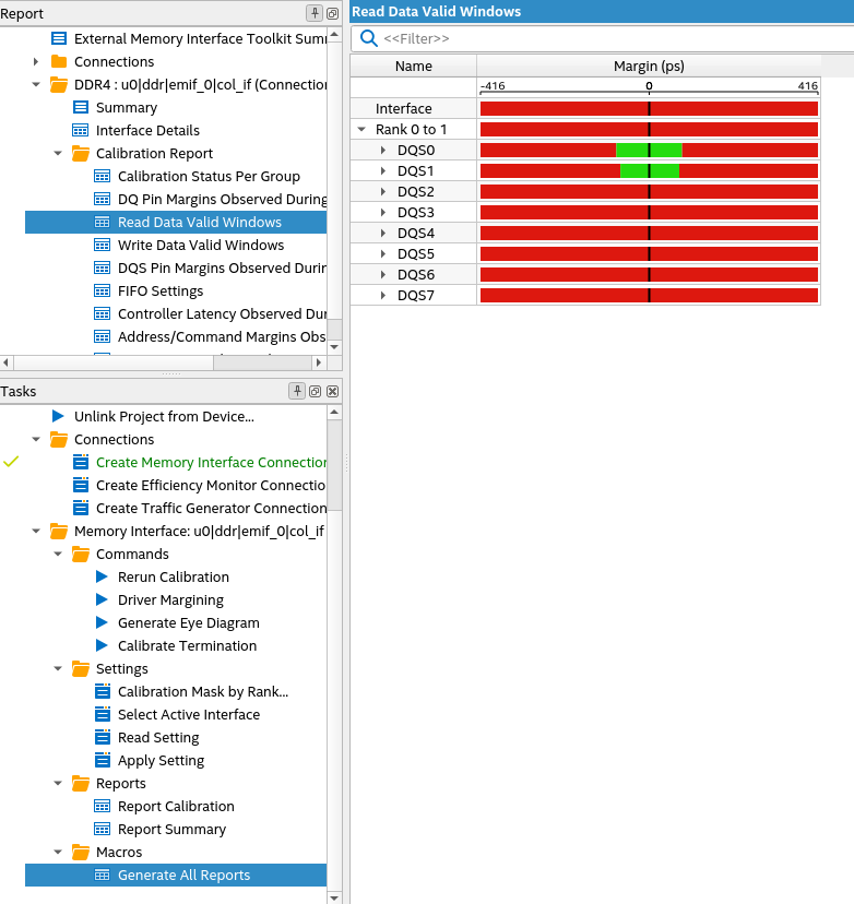
Unfortunately, I got an error on calibration stage. After some timing fixes using RAM chip datasheet, I got a passed Write Leveling stage, but fails on Read Per-bit Deskew (see attached screenshots).
For this specific project, I need to use DDR4 2400MHz UDIMM 2Rx8 Non-ECC memory. Does Arria 10 support such type of memories? For some reason, I haven't found any example design for UDIMM 2-rank memory to compare settings and timings.
Quartus Prime version - 21.1.0 Build 169 Pro Edition.
- Mark as New
- Bookmark
- Subscribe
- Mute
- Subscribe to RSS Feed
- Permalink
- Report Inappropriate Content
Hello Mark,
I have attached the example design in .qar file below. Please let me know if this design can fit into your board.
Please share the Report DDR as snapshot below after the compilation process.

Link Copied
- Mark as New
- Bookmark
- Subscribe
- Mute
- Subscribe to RSS Feed
- Permalink
- Report Inappropriate Content
Hello Mark,
The Arria 10 device can support DDR4 memory device with UDIMM memory format , up to 2 DIMM per channel , up to 4 Rank topologies.
You can check the details with EMIF Spec Estimator in this link: https://www.intel.com/content/www/us/en/support/programmable/support-resources/support-centers/emif-spec-estimator.html
I can help to check the EMIF IP configuration based on the memory device datasheet.
Can you share the memory device datasheet that you are using and also some snapshots of the EMIF IP?
Thanks & Regards,
Adzim
- Mark as New
- Bookmark
- Subscribe
- Mute
- Subscribe to RSS Feed
- Permalink
- Report Inappropriate Content
Hello.
Currently I am using the following memories:
| Kingston | KVR26N19D8/16 | Samsung K4A8G085WE-BCWE | 16 GB | 2666 | UDIMM | 2Rx8 | Non-ECC |
| SK hynix | HMA82GU6AFR8N-UH | SK hynix H5AN8G8NAFR-UHC | 16 GB | 2400 | UDIMM | 2Rx8 | Non-ECC |
Here are manuals from memory manufacturer:
https://www.memory-distributor.com/pub/media/downloads/datasheets/K4A8Gxx5WC.pdf
https://download.datasheets.com/pdfs/2017/11/3/5/12/58/809/hyn_/manual/h5an8g6nafr-vkc.pdf
So far, I have reached pretty good marging, but it started to fail write leveling after 2nd group.
Attaching zip archive with calibration results and EMIF parameters.
- Mark as New
- Bookmark
- Subscribe
- Mute
- Subscribe to RSS Feed
- Permalink
- Report Inappropriate Content
Hello Mark,
Thank you for sharing the datasheets.
I have checked the EMIF IP setting with the memory datasheets and there are some settings that are not accurate.
I will attach the file that contain the snapshot of the EMIF IP setting.
Please let me know if you have any question.
Regards,
Adzim
- Mark as New
- Bookmark
- Subscribe
- Mute
- Subscribe to RSS Feed
- Permalink
- Report Inappropriate Content
Hello Adzim,
Unfortunately, EMIF IP configs from your file didn't solve the calibration issue. I will attach the results in another .zip file.
- Mark as New
- Bookmark
- Subscribe
- Mute
- Subscribe to RSS Feed
- Permalink
- Report Inappropriate Content
Hello Mark,
Do you see any timing violation in the Compilation report?
Especially in "emif_0|emif_0 " table that you can find in Timing Analyzer/Report DDR/*all model*
Are you using the example design or your own design?
The pin placement for address/command pins must be followed "DDR4 Scheme 4: Component/UDIMM/RDIMM".
I think the alert_n signal is suitable to be placed along with the DQS group.
Can you check the pin placement as well?
Regards,
Adzim
- Mark as New
- Bookmark
- Subscribe
- Mute
- Subscribe to RSS Feed
- Permalink
- Report Inappropriate Content
Hello Mark,
Do you have any feedback in this thread?
Regards,
Adzim
- Mark as New
- Bookmark
- Subscribe
- Mute
- Subscribe to RSS Feed
- Permalink
- Report Inappropriate Content
Hello Adzim,
Sorry for delayed answer. I had no time to check it on previous week.
I will attach Timing Analyzer results to this message. I believe, it says the same thing that I see from EMIF Debugger. I haven't tried to use this tool before, so I might miss something from it.
The project is based on example design with modified parameters.
Also, I am pretty sure that pins are correct, because the same project with different timings in EMIF IP has been used with different memories like UDIMM 1Rx8 non-ECC, RDIMM 2Rx8 ECC etc.
Best regards,
Mark
- Mark as New
- Bookmark
- Subscribe
- Mute
- Subscribe to RSS Feed
- Permalink
- Report Inappropriate Content
Hi Mark,
There is timing violation in your design. This will cause the failure during the calibration process.
May I know the device OPN that you used? And can you provide the pin placement as well?
I will try to generate an example design and share with you for debugging purpose.
Thanks,
Adzim
- Mark as New
- Bookmark
- Subscribe
- Mute
- Subscribe to RSS Feed
- Permalink
- Report Inappropriate Content
Hello Adzim,
I am using an unique board with installed FPGA that was developed by my company, so I cannot give much details about it.
Attaching pin planner .csv file.
Best regards,
Mark
- Mark as New
- Bookmark
- Subscribe
- Mute
- Subscribe to RSS Feed
- Permalink
- Report Inappropriate Content
Hello Mark,
I have attached the example design in .qar file below. Please let me know if this design can fit into your board.
Please share the Report DDR as snapshot below after the compilation process.
- Mark as New
- Bookmark
- Subscribe
- Mute
- Subscribe to RSS Feed
- Permalink
- Report Inappropriate Content
Hello Adzim,
I have tested example design from your project. EMIF IP settings are working on my board. All 6 same type RAMs from different vedors have passed calibration.
Also, I tried to increase working frequency up to 1200MHz and it was still working. It took me around 1 month to find a proper settings and your solution finally give me a required result.
Do you have any hints that might help me to find a similar solution for different RAM types in the future?
Thank you very much for help!
Best regards,
Mark


- Mark as New
- Bookmark
- Subscribe
- Mute
- Subscribe to RSS Feed
- Permalink
- Report Inappropriate Content
Hi Mark,
I am glad to hear that your memory devices are passing the calibration.
I hope that you can move forward with this success.
Below are some hints that can help to configure the DDR in future :-
- Always check the Calibration Report for any violation especially in timing analysis.
- Double check the EMIF IP setting with memory device datasheet.
- Refer to DDR scheme when placing the pin in IO Bank.
- Testing with EMIF example design first.
I will transition this thread into community support. Feel free to open a new thread if you have a new question. Otherwise, the community users will continue to help you on this thread.
Thank you.
Regards,
Adzim
- Subscribe to RSS Feed
- Mark Topic as New
- Mark Topic as Read
- Float this Topic for Current User
- Bookmark
- Subscribe
- Printer Friendly Page