- Mark as New
- Bookmark
- Subscribe
- Mute
- Subscribe to RSS Feed
- Permalink
- Report Inappropriate Content
Dear friends,
I'm using MAX10 (10M08DAF484C8GES), Quartus 18.1 and On-Chip Flash Intel FPGA IP.
My problem is:
When I need erase Sector ID1 or ID2 (or another), the "busy" from Core status Register goes to High (2'b01 BUSY_ERASE) and next clock goes to Low (2'b00 IDLE). But the "es (erase successful)" is Low (1'b0 Erase failed). What can i do?
wp (Sector ID x write protection) is disable, sp (Sector ID 1 protection bit) is Low to (I can't setup, but I read 0).
It's normaly, when "busy" goes High (BUSY_ERASE) and next clock goes Low (IDDLE)?
My simplified code:
erase_state: process(PIN_OSCILATOR)
begin
if(rising_edge(PIN_OSCILATOR)) then
if(flagErase='1') then
actionErase<='1';
end if;
case stateErase is
when ERASE_READSTATUS_A_ON =>
flashConfigAddr<='0'; --Status register
flashConfigRead<='1';
stateErase<=ERASE_READSTATUS_A_OFF;
when ERASE_READSTATUS_A_OFF =>
flashConfigRead<='0';
stateErase<=ERASE_READSTATUS_A_VALUE;
when ERASE_READSTATUS_A_VALUE =>
flashStatus<=flashConfigReadData(9 downto 0);
stateErase<=ERASE_DISABLEWP_ON;
when ERASE_DISABLEWP_ON =>
if(flashStatus(1 downto 0)="00") then --Idle
flashConfigAddr<='1'; --Control register
flashConfigWrite<='1';
flashConfigWritedata<="11111110011111111111111111111111"; --Disable write protected mode Sector ID1, ID2
stateErase<=ERASE_DISABLEWP_OFF;
else
stateErase<=ERASE_READSTATUS_A_ON; --busy, testing again
end if;
when ERASE_DISABLEWP_OFF =>
flashConfigWrite<='0';
stateErase<=ERASE_READSTATUS_B_ON;
when ERASE_READSTATUS_B_ON =>
flashConfigAddr<='0'; --Status register
flashConfigRead<='1';
stateErase<=ERASE_READSTATUS_B_OFF;
when ERASE_READSTATUS_B_OFF =>
flashConfigRead<='0';
stateErase<=ERASE_READSTATUS_B_VALUE;
when ERASE_READSTATUS_B_VALUE =>
flashStatus<=flashConfigReadData(9 downto 0);
stateErase<=ERASE_ERASECFM2_ON;
when ERASE_ERASECFM2_ON =>
if(flashStatus(1 downto 0)="00") then --Idle
flashConfigAddr<='1'; --Control register
flashConfigWrite<='1';
flashConfigWritedata<="11111111100111111111111111111111"; --Erase Sector ID1 (UFM1)
stateErase<=ERASE_ERASECFM2_OFF;
else
stateErase<=ERASE_READSTATUS_B_ON; --busy, testing again
end if;
when ERASE_ERASECFM2_OFF =>
flashConfigWrite<='0';
stateErase<=ERASE_READSTATUS_C_ON;
when ERASE_READSTATUS_C_ON =>
flashConfigAddr<='0'; --Status register
flashConfigRead<='1';
stateErase<=ERASE_READSTATUS_C_OFF;
when ERASE_READSTATUS_C_OFF =>
flashConfigRead<='0';
stateErase<=ERASE_READSTATUS_C_VALUE;
when ERASE_READSTATUS_C_VALUE =>
flashStatus<=flashConfigReadData(9 downto 0);
stateErase<=ERASE_ERASECFM1_ON;
when ERASE_ERASECFM1_ON =>
if(flashStatus(1 downto 0)="00") then --Idle
flashConfigAddr<='1'; --Control register
flashConfigWrite<='1';
flashConfigWritedata<="11111111101011111111111111111111"; --Erase Sector ID2 (UFM0)
stateErase<=ERASE_ERASECFM1_OFF;
else
stateErase<=ERASE_READSTATUS_C_ON; --busy, testing again
end if;
when ERASE_ERASECFM1_OFF =>
flashConfigWrite<='0';
stateErase<=ERASE_READSTATUS_D_ON;
when ERASE_READSTATUS_D_ON =>
flashConfigAddr<='0'; --Status register
flashConfigRead<='1';
stateErase<=ERASE_READSTATUS_D_OFF;
when ERASE_READSTATUS_D_OFF =>
flashConfigRead<='0';
stateErase<=ERASE_READSTATUS_D_VALUE;
when ERASE_READSTATUS_D_VALUE =>
flashStatus<=flashConfigReadData(9 downto 0);
stateErase<=ERASE_ENABLEWP_ON;
when ERASE_ENABLEWP_ON =>
if(flashStatus(1 downto 0)="00") then --Idle
flashConfigAddr<='1'; --Control register
flashConfigWrite<='1';
flashConfigWritedata<="11111111111111111111111111111111"; --Enable write protected mode Sector ID2, ID1 (UFM1, UFM0)
stateErase<=ERASE_ENABLEWP_OFF;
else
stateErase<=ERASE_READSTATUS_D_ON; --busy, testing again
end if;
when ERASE_ENABLEWP_OFF =>
flashConfigWrite<='0';
stateErase<=ERASE_READSTATUS_E_ON;
when ERASE_READSTATUS_E_ON =>
flashConfigAddr<='0'; --Status register
flashConfigRead<='1';
stateErase<=ERASE_READSTATUS_E_OFF;
when ERASE_READSTATUS_E_OFF =>
flashConfigRead<='0';
stateErase<=ERASE_READSTATUS_E_VALUE;
when ERASE_READSTATUS_E_VALUE =>
flashStatus<=flashConfigReadData(9 downto 0);
stateErase<=ERASE_FINISH;
when ERASE_FINISH =>
if(flashStatus(1 downto 0)="00") then --Idle
stateErase<=ERASE_STANDBY;
else
stateErase<=ERASE_READSTATUS_E_ON; --busy, testing again
end if;
when ERASE_STANDBY =>
if (actionErase='1') then
stateErase<=ERASE_READSTATUS_A_ON;
actionErase<='0';
else
stateErase<=ERASE_STANDBY;
flashConfigWrite<='0';
flashConfigRead<='0';
flashStatus<= (others=>'0');
end if;
end case;
end if;
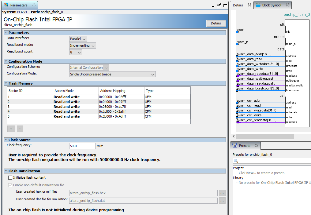
end process erase_state;I send IP setting and Scope signals (Read and Write signals are avmm_csr_read and avmm_csr_write, next signals are Core Status Register from flashStatus on my code).
Thank you, Tomas
Link Copied
- Mark as New
- Bookmark
- Subscribe
- Mute
- Subscribe to RSS Feed
- Permalink
- Report Inappropriate Content
Hi ,
Can you please check the figure 11 and 12 wave form of the below document correlates with your finding .
https://www.intel.com/content/dam/www/programmable/us/en/pdfs/literature/hb/max-10/ug_m10_ufm.pdf
- Mark as New
- Bookmark
- Subscribe
- Mute
- Subscribe to RSS Feed
- Permalink
- Report Inappropriate Content
Dear,
thank you for your answer. Figure 11 and 12 is Read Operation. It working good [when I use "non-default initialization file" on "On-Chip Flash IntelFPGA IP", the data stored via USB Blaster I read via "On-Chip Flash IntelFPGA IP (figure 11 and 12 on your answer)" good].
I can't erasing. I can't find any erasing figure or example, only 4.2.4. and 4.2.5. on your document.
When i disable the write protection, then test BUSY state (=IDLE). Then I write erase operation in the status register. Then test BUSY state. BUSY state is BUSY_ERASE now, but only one clock period. Next clock period is BUSY reading IDLE again. Flash is no erased and es (erase successful) is 1'b0 always.
I don't know what I doing wrong..
Thank you, Tomas
- Mark as New
- Bookmark
- Subscribe
- Mute
- Subscribe to RSS Feed
- Permalink
- Report Inappropriate Content
SOLVED,
my bad sequence:
flashConfigWritedata<="11111110011111111111111111111111"; --Disable write protected mode Sector ID1, ID2
flashConfigWritedata<="11111111100111111111111111111111"; --Erase Sector ID1 (UFM1) *write protected is enabled again - bad!!
flashConfigWritedata<="11111111101011111111111111111111"; --Erase Sector ID2 (UFM0) *write protected is enabled again - bad!!
flashConfigWritedata<="11111111111111111111111111111111"; --Enable write protected mode Sector ID2, ID1 (UFM1, UFM0)
good sequence:
flashConfigWritedata<="11111110011111111111111111111111"; --Disable write protected mode Sector ID1, ID2
flashConfigWritedata<="11111110000111111111111111111111"; --Erase Sector ID1 (UFM1) *write protected is disabled permanently- good!!
flashConfigWritedata<="11111110001011111111111111111111"; --Erase Sector ID2 (UFM0) *write protected is disabled permanently- good!!
flashConfigWritedata<="11111111111111111111111111111111"; --Enable write protected mode Sector ID2, ID1 (UFM1, UFM0)
Tomas
- Subscribe to RSS Feed
- Mark Topic as New
- Mark Topic as Read
- Float this Topic for Current User
- Bookmark
- Subscribe
- Printer Friendly Page