- Mark as New
- Bookmark
- Subscribe
- Mute
- Subscribe to RSS Feed
- Permalink
- Report Inappropriate Content
hi,
i use the civgx30 on my board to utilize the pciex4 hardip. but unfortunately,i connect (slot lane0) to (fpga lane3),and (slot lane1) to (fpga lane2),and (slot lane2) to (fpga lane1), and (slot lane3) to (fpga lane0). so ,my board cant work. software i use the quartus 11.1. do anyone have some idea? thanks!Link Copied
- Mark as New
- Bookmark
- Subscribe
- Mute
- Subscribe to RSS Feed
- Permalink
- Report Inappropriate Content
no reply ?
- Mark as New
- Bookmark
- Subscribe
- Mute
- Subscribe to RSS Feed
- Permalink
- Report Inappropriate Content
I just came across your post because I was reviewing documents about the lane reversal feature of the PCIe hard IP core for Cyclone V. According to the PCIe user guide, Cyclone IV hard IP also does support lane reversal.
But does it actually work, and is it automatical or must it be configured? Unlike Arria V, that has a pin assignment perfectly ordered for a PCIe card, Cyclone V needs lane reversal if you don't want to cross all Rx and Tx pairs in a 4 lane design.- Mark as New
- Bookmark
- Subscribe
- Mute
- Subscribe to RSS Feed
- Permalink
- Report Inappropriate Content
Simply pin-out the FPGA correctly (0 to 0, 1 to 1, 2 to 2, 3 to 3). The Ip will functionally then perform Lane Reversal Automatically for you. This is a built in required feature of PCIe.
- Mark as New
- Bookmark
- Subscribe
- Mute
- Subscribe to RSS Feed
- Permalink
- Report Inappropriate Content
Thank you for the clarification. I got the same answer from Altera support in the meantime, also regarding keeping the regular PCIe pinout in Quartus (which I didn't consider before).
This is good news, because it allows a straightforward routing of a standard PCIe x4 interface.- Mark as New
- Bookmark
- Subscribe
- Mute
- Subscribe to RSS Feed
- Permalink
- Report Inappropriate Content
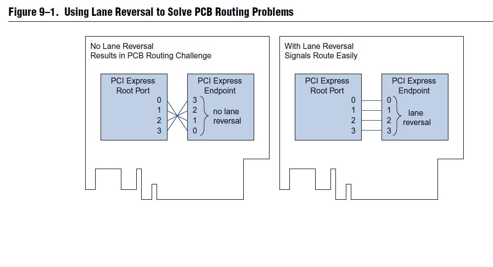
--- Quote Start --- Simply The Ip will functionally then perform Lane Reversal Automatically for you. This is a built in required feature of PCIe. --- Quote End --- What do You mean - pin-out the FPGA correctly (0 to 0, 1 to 1, 2 to 2, 3 to 3)? According to the attached picture 0 to 0, 1 to 1, 2 to 2, 3 to 3 can be both for Plane reversal and No plane reversal. How exactly is to make plane reversal for Cyclone IV GX with PCIe x 4 Hard IP? Apparently that has to be done in *.qsf file, in Pin Planner or where?
- Mark as New
- Bookmark
- Subscribe
- Mute
- Subscribe to RSS Feed
- Permalink
- Report Inappropriate Content
For clarification, see the full answer from Altera Support.
The point is to understand the difference between Quartus pinout and PCB wiring. --- Quote Start --- Q1) Is Lane Reversal available for a x4 endpoint interface, e.g. a PCIe card A1) Yes. Q2) I don't exactly understand the assignment options addressed with table 12-4 Lane Assignments with Lane Reversal. Does it mean that a reversed order of both Rx and Tx pairs is supported? A2) The documentation means that user can do lan reversal on both RX and TX pair. For example for a x4 lane, you can route your board transmitter and receiver Lane3 to the edge connector Lane0, transmitter and receiver Lane2 to Lane1 and so on. Q3) Referring to figure Figure 7–38, we connect PCI Express Lane 0 to Transceiver channel 3, Lane 1 to channel 2, Lane 2 to channel 1 and Lane 3 to channel 0? A3) No. You still need to connect in a non-reverse order to the transceiver (during Quartus II pin assignment). For reversal, you need to do it when you route your PCB board tx/rx pair to the PCIe edge connector as explained in A2. Q4) How to activate lane reversal? Or is it automatic? A4) Yes, it is automatic. --- Quote End ---- Mark as New
- Bookmark
- Subscribe
- Mute
- Subscribe to RSS Feed
- Permalink
- Report Inappropriate Content
What document are You refering to for table 12-4 and Figure 7–38?
What was the SR reply about - Cyclone V or IV?- Mark as New
- Bookmark
- Subscribe
- Mute
- Subscribe to RSS Feed
- Permalink
- Report Inappropriate Content
It's about CV. I'm not familiar with CIV hard IP. If the specification says it supports lane reversal, I would expect the information is valid for CIV as well.
- Mark as New
- Bookmark
- Subscribe
- Mute
- Subscribe to RSS Feed
- Permalink
- Report Inappropriate Content
--- Quote Start --- for reversal, you need to do it when you route your pcb board tx/rx pair to the pcie edge connector as explained in a2. --- Quote End --- What is A2? I did not find it in Cyclone V Hard IP for PCI Express User Guide.
- Mark as New
- Bookmark
- Subscribe
- Mute
- Subscribe to RSS Feed
- Permalink
- Report Inappropriate Content
A2 means Answer 2 in the support solution.
- Mark as New
- Bookmark
- Subscribe
- Mute
- Subscribe to RSS Feed
- Permalink
- Report Inappropriate Content
It seems, that for Altera support terms "route" and "connect" mean different things.
What is wrong then with what did the topicstarter: (slot lane0) to (fpga lane3),and (slot lane1) to (fpga lane2),and (slot lane2) to (fpga lane1), and (slot lane3) to (fpga lane0)? If this is the way he "routed" the PCB, then it is correct? But if this is the way he "connected" in Quartus pin assignment, then it is not correct? Did I understand correctly the answer from Altera support?- Mark as New
- Bookmark
- Subscribe
- Mute
- Subscribe to RSS Feed
- Permalink
- Report Inappropriate Content
one more question here: I do not understand why the x4 core lane reversal has to do with the slot size.
does this means we have to get to know the root complex (link partner) size slot size before we route the reversed lanes on end point size PCB?

- Subscribe to RSS Feed
- Mark Topic as New
- Mark Topic as Read
- Float this Topic for Current User
- Bookmark
- Subscribe
- Printer Friendly Page