- Mark as New
- Bookmark
- Subscribe
- Mute
- Subscribe to RSS Feed
- Permalink
- Report Inappropriate Content
I have designed and data acquisition card. it uses pcie x4 interface to communacate with the host computer.
the card is base on an cyclone iv gx 50 F672 fpga device, the quartus ii software version is 11.1. I generated the pcie ip core with the megacore function tool. the pcie refclk pins use fpga's refclk0p/n, PIN_T9 and PIN_U9. the complication is error. why? please help me.Link Copied
9 Replies
- Mark as New
- Bookmark
- Subscribe
- Mute
- Subscribe to RSS Feed
- Permalink
- Report Inappropriate Content
Provide more information about error. Give the console log output, pin assignments, core settings, interconnect screenshot, etc. Nobody will help You having no information except: "ERROR. WHY?"...
- Mark as New
- Bookmark
- Subscribe
- Mute
- Subscribe to RSS Feed
- Permalink
- Report Inappropriate Content
Thanks for Socrates's reply.
my problem is below: compilation succeeds pin assignment: ...... set_location_assignment pin_t14 -to refclk set_location_assignment pin_t15 -to "refclk(n)" set_location_assignment PIN_AA2 -to rx_in0 set_location_assignment PIN_W2 -to rx_in1 set_location_assignment PIN_U2 -to rx_in2 set_location_assignment PIN_R2 -to rx_in3 set_location_assignment PIN_Y4 -to tx_out0 set_location_assignment PIN_V4 -to tx_out1 set_location_assignment PIN_T4 -to tx_out2 set_location_assignment PIN_P4 -to tx_out3 compilation failed pin assignment: set_location_assignment pin_t9 -to refclk set_location_assignment pin_u9 -to "refclk(n)" set_location_assignment PIN_AA2 -to rx_in0 set_location_assignment PIN_W2 -to rx_in1 set_location_assignment PIN_U2 -to rx_in2 set_location_assignment PIN_R2 -to rx_in3 set_location_assignment PIN_Y4 -to tx_out0 set_location_assignment PIN_V4 -to tx_out1 set_location_assignment PIN_T4 -to tx_out2 set_location_assignment PIN_P4 -to tx_out3 the error message: Info (167065): Input frequency of fixedclk for the GXB Central Control Unit "ip_pciex4_example_chaining_pipen1b:core|ip_pciex4_plus:ep_plus|ip_pciex4:epmap|ip_pciex4_serdes:serdes|ip_pciex4_serdes_alt_c3gxb_7ue8:ip_pciex4_serdes_alt_c3gxb_7ue8_component|cent_unit0" must be 125.0 MHz error (176559): can't place mpll or gpll pll "ip_pciex4_example_chaining_pipen1b:core|ip_pciex4_plus:ep_plus|ip_pciex4:epmap|ip_pciex4_serdes:serdes|ip_pciex4_serdes_alt_c3gxb_7ue8:ip_pciex4_serdes_alt_c3gxb_7ue8_component|altpll:pll0|altpll_nn81:auto_generated|pll1" in pll location pll_5 because i/o cell "refclk" cannot be placed in i/o pin pin_t9 (port type inclk of the pll) Info (171121): Fitter preparation operations ending: elapsed time is 00:00:02 Warning (171167): Found invalid Fitter assignments. See the Ignored Assignments panel in the Fitter Compilation Report for more information. Error (171000): Can't fit design in device Warning (169177): 2 pins must meet Altera requirements for 3.3-, 3.0-, and 2.5-V interfaces. For more information, refer to AN 447: Interfacing Cyclone IV GX Devices with 3.3/3.0/2.5-V LVTTL/LVCMOS I/O Systems. Info (169178): Pin pcie_rstn uses I/O standard 3.3-V LVCMOS at U19 Info (169178): Pin local_rstn_ext uses I/O standard 3.3-V LVCMOS at W26 Error: Quartus II 32-bit Fitter was unsuccessful. 2 errors, 14 warnings Error: Peak virtual memory: 335 megabytes Error: Processing ended: Sun Jan 29 10:47:12 2012 Error: Elapsed time: 00:00:12 Error: Total CPU time (on all processors): 00:00:10 Error (293001): Quartus II Full Compilation was unsuccessful. 4 errors, 535 warnings but, my card select the failed pin assignment. please help fix the problem.- Mark as New
- Bookmark
- Subscribe
- Mute
- Subscribe to RSS Feed
- Permalink
- Report Inappropriate Content
who can help me?
please stand up!- Mark as New
- Bookmark
- Subscribe
- Mute
- Subscribe to RSS Feed
- Permalink
- Report Inappropriate Content
Well, I haven't have such issue, but the error is pretty self-explained. The clock has a wrong frequency (requires 125MHz). And double check the pin assignments.
- Mark as New
- Bookmark
- Subscribe
- Mute
- Subscribe to RSS Feed
- Permalink
- Report Inappropriate Content
pcie接口
Rx0-4、Tx0-4 REFCLK 使用Quartus 11.1的MegaWizard Plug-in Manager工具生成IP Compiler for Pcie Express V11.1。 在Quartus 11.1中对自动生成的工程进行编译,没有进行管脚绑定时,能够通过编译。 使用如下管脚绑定能够通过编译。 set_location_assignment PIN_T14 -to refclk set_location_assignment PIN_T15 -to "refclk(n)" set_location_assignment PIN_AA2 -to rx_in0 set_location_assignment PIN_W2 -to rx_in1 set_location_assignment PIN_U2 -to rx_in2 set_location_assignment PIN_R2 -to rx_in3 set_location_assignment PIN_Y4 -to tx_out0 set_location_assignment PIN_V4 -to tx_out1 set_location_assignment PIN_T4 -to tx_out2 set_location_assignment PIN_P4 -to tx_out3 使用如下管脚绑定不能够通过编译。 set_location_assignment PIN_T9 -to refclk set_location_assignment PIN_U9 -to "refclk(n)" set_location_assignment PIN_AA2 -to rx_in0 set_location_assignment PIN_W2 -to rx_in1 set_location_assignment PIN_U2 -to rx_in2 set_location_assignment PIN_R2 -to rx_in3 set_location_assignment PIN_Y4 -to tx_out0 set_location_assignment PIN_V4 -to tx_out1 set_location_assignment PIN_T4 -to tx_out2 set_location_assignment PIN_P4 -to tx_out3 问题在于通过编译的管脚绑定使用了REFCLK2,PCIE差分参考时钟经GPLL_1、MPLL_5,再用于PCIE CORE,而未通过编译的管脚绑定使用了REFCLK0、REFCLK1,PCIE差分参考时钟没有经过GPLL_1。 而我们的设计恰好将PCIE差分参考时钟绑定到REFCLK0,造成逻辑加载后没有任何反应。 编译器报错如下: Error (176559): Can't place MPLL or GPLL PLL "ip_pciex4_example_chaining_pipen1b:core|ip_pciex4_plus:ep_plus|ip_pciex4:epmap|ip_pciex4_serdes:serdes|ip_pciex4_serdes_alt_c3gxb_7ue8:ip_pciex4_serdes_alt_c3gxb_7ue8_component|altpll:pll0|altpll_nn81:auto_generated|pll1" in PLL location PLL_5 because I/O cell "refclk" cannot be placed in I/O pin Pin_T9 (port type INCLK of the PLL)。 具体图见附件。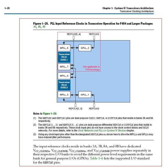
- Mark as New
- Bookmark
- Subscribe
- Mute
- Subscribe to RSS Feed
- Permalink
- Report Inappropriate Content
from the attachment picture:
I can see that the successful compilation pcie ip core uses the refclk2 clock pins, the pcie refclk inputs to the pll_1. the failed compilation pcie ip core uses the refclk0 clock pins, the pcie refclk inputs to the pll_5. the two verisions are different from the pll_1 and pll_5. the default pcie core uses the pll_1. but i want to use the pll_5. how can i do this?- Mark as New
- Bookmark
- Subscribe
- Mute
- Subscribe to RSS Feed
- Permalink
- Report Inappropriate Content
Hi Zlfeng1110
Did you solve your issue? I have a similar issue. From the Cyclone IV Transceiver Architecture Fig 1-26, it looks like we should be using MPLL_5 with input pins REFCLK[1,0]. Cheers- Mark as New
- Bookmark
- Subscribe
- Mute
- Subscribe to RSS Feed
- Permalink
- Report Inappropriate Content
oh,my god,i have the same question.did you solve it now?
- Mark as New
- Bookmark
- Subscribe
- Mute
- Subscribe to RSS Feed
- Permalink
- Report Inappropriate Content
Hello, I know I'm quite late to the rest of the posts, but I had the same problem and have solved it.
The problem is the assignment of the reference clock and the PLL clock: -The reference clock is used for calibration (cal_blk_clk) -The PLL clock is used to generate the transceiver main clock (pll_inclk) these two clock may not be from the same source!
Even if the frequencies are appropriate for both clock inputs, they come from different sources! The reference clock has its own dedicated refclk pin. Please make sure you use only this pin for the cal_blk_clk. Make sure you use this pin for nothing else! The error message should be more informative, but if you read about the transceiver architecture of your device you will understand why these two clocks must come from separate sources. Even if you leave the software to automatically select pin locations, your schematic/HDL must not have these two clock inputs come from the same source. There is nothing the fitter can do if you have them originate from the same source since the design is impossible to fit.
Reply
Topic Options
- Subscribe to RSS Feed
- Mark Topic as New
- Mark Topic as Read
- Float this Topic for Current User
- Bookmark
- Subscribe
- Printer Friendly Page