- Mark as New
- Bookmark
- Subscribe
- Mute
- Subscribe to RSS Feed
- Permalink
- Report Inappropriate Content
Hi,
After the following discussion and some email communication,
https://forums.intel.com/s/question/0D50P00004UIHagSAH/an881-reference-design-need-to-be-upgraded-for-device-1sm21ch,
AN881 design still cannot work on our board (16GB HBM2 version).
Above discussion has been closed, so I create a new one.
Let me summarize the experiment results so far,
- Compile AN881 by Quartus 18.1 or 19.1, and change device to 1SM21CHU1F53E1VG. Linux server cannot recognize FPGA (by lspci command).
- Compile AN881 by Quartus 19.3, and change device to 1SM21CHU1F53E1VG. There are some error message when upgrading IP process.
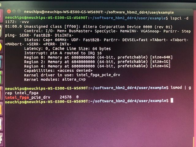
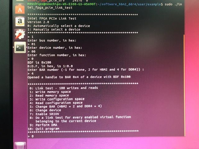
- Compile AN881 by Quartus 19.2, and change device to 1SM21CHU1F53E1VG. Linux server can recognize FPGA PCIe device by lspci command, and the BAR memory space is allocated by BIOS successfully. However, the test program (software_hbm2_ddr4 folder included in AN881) always fails. The driver is installed successfully, but once we execute "link test" or "DMA test" function, the Linux system crashes so that we need to restart the computer. As attached figure, when we enter 0 to choose "0: Link test", the system doesn't response anymore.
In previous discussion by e-mail, AN881 design author said the design works on Intel's side.
However, their device is not 1SM21CHU*.
Every time we change the device setting to 1SM21CHU*, it doesn't work.
Link Copied
- Mark as New
- Bookmark
- Subscribe
- Mute
- Subscribe to RSS Feed
- Permalink
- Report Inappropriate Content
Hi Sir,
I am sorry for the inconvenience caused.
I understand that you borrow the BHU board from someone. May I know that when using the BHU board, is this design working?
Also, the AN881 has been updated, especially section 2.2.
https://www.intel.com/content/dam/www/programmable/us/en/pdfs/literature/an/an881.pdf#page=11
You have to run some post processing after re-generate the IP.
- Mark as New
- Bookmark
- Subscribe
- Mute
- Subscribe to RSS Feed
- Permalink
- Report Inappropriate Content
Hi,
The BHU board works.
Actually, the board is not at our hand,
the selling agent (i.e. Arrow) borrowed it from Intel Shanhai site, and returned the board after testing recently.
Arrow tell us the design works on BHU board.
I'll try the post-processing again,
but I remember that I've tried the script in previous experiments.
Thanks.
- Mark as New
- Bookmark
- Subscribe
- Mute
- Subscribe to RSS Feed
- Permalink
- Report Inappropriate Content
Please give it a try with the post-processing again. This is a must step if re-generate the Qsys.
By the way, can I get some clarification from you:-
1. In the screen shot capture you are targeting DDR4, is it expected? In this case, I assume the DDR4 DIMM is slot in to the board right? We need to ensure the DDR4 is calibrated successfully. Can you assign the DDR4 calibration status signal to an indicator like LED or signaltap?
2. Did you change the design like BARs size etc? I assume you direct upgrade the design from BHU to CHU, run the post processing script and did not make any modification right?
If the issue still persist after run the post processing script, is it possible to send the design to mefor review? Thanks
- Mark as New
- Bookmark
- Subscribe
- Mute
- Subscribe to RSS Feed
- Permalink
- Report Inappropriate Content
Hi,
I try the script today, but the result is still the same.
1.
We expect to use both DDR4 and HBM2, but either DDR or HBM2 failed.
And yes, DDR4 DIMM is in the FPGA board.
I think the root cause is related to PCIe gen3x16, not DDR4.
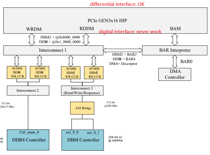
Because PCIe controller didn't sent any request to DDR/HBM according to SignalTap, although Linux can recognize PCIe and BIOS can allocate BAR memory space.
There must be something wrong inside PCIe hard IP+.
i.e. RDDM/WRDM/BAM interface never toggle during testing.
2.
No, we didn't change BAR size. As you said, we only upgrade the design and run script, then start the compilation.
We attach the project files, please review it.
It would be better if you can get a CHU board and trying this design.
I thought Intel should provide a board to you, but I don't know why it's difficult to get a CHU board inside Intel during previous discussion and experiments.
Thank you.
- Subscribe to RSS Feed
- Mark Topic as New
- Mark Topic as Read
- Float this Topic for Current User
- Bookmark
- Subscribe
- Printer Friendly Page


