- Mark as New
- Bookmark
- Subscribe
- Mute
- Subscribe to RSS Feed
- Permalink
- Report Inappropriate Content
Hello everybody
Taking a look to the schematic of the Arrow BeMicro MAX 10 tool I could see a connector labeled "USB_Blaster_JTAG" (J7). Then looking for images of the tool I can see that this is not exactly a connector but is 5 exposed pads at the edge of the PCB and I assume they are distributed as the labels in the image taking as a reference the little "triangle" which I think indicates PIN1. http://www.alteraforum.com/forum/attachment.php?attachmentid=11279&stc=1 I haven't found images for the bottom of the tool but I assume that I could find the other 5 pads at the bottom side. As I have a MAX 10 FPGA Evaluation kit from Altera and I didn't buy the usb blaster as a bundle (huge mistake), I would like to know if I can use this BeMicro tool as a USB blaster to program my "MAX 10 FPGA Evaluation kit" since I don't want to spend $300 usd in a USB blaster specially if I can have one for $30 (being part of a tool that I also need). Could anyone confirm this please? I'll appreciate it. Regards.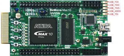
Link Copied
6 Replies
- Mark as New
- Bookmark
- Subscribe
- Mute
- Subscribe to RSS Feed
- Permalink
- Report Inappropriate Content
Check the schematics ...
http://www.alterawiki.com/uploads/e/ec/bemicro_max_10-schematic_a4-20141008.pdf Page 6 shows the header details. There appears to be two JTAG interfaces; the 6-pin header for programming the MAXV CPLD and the edge connector for ... what? You cannot tell what this port is for. Its most likely for attaching an external USB-Blaster that is then passed through the MAXV to the JTAG side of the MAX10 device. Before connecting to the edge pads, try to figure out what direction the pins are configured for. I doubt the source is provided for the MAXV device. I'd recommend buying at Terasic USB-Blaster for $50. They are identical to the $300 Altera USB-Blasters. Cheers, Dave- Mark as New
- Bookmark
- Subscribe
- Mute
- Subscribe to RSS Feed
- Permalink
- Report Inappropriate Content
Hey,
The port J7 is actually a cool feature. It allows to you steer the JTAG to program the external device instead of the on board MAX10. There's a voltage detect pin signal that goes to the CPLD and the CPLD steers the Blaster to the J7 header. Then you'd have a cheaper USB-Blaster for 30bucks :D Jeff- Mark as New
- Bookmark
- Subscribe
- Mute
- Subscribe to RSS Feed
- Permalink
- Report Inappropriate Content
jefflieu thanks for helping!
So, can I use this tool as a USB blaster to program another tool connecting it as in the attached image? Or, do you have a diagram with J7 pin out that shows how can I use it as a USB blaster? Thanks!!- Mark as New
- Bookmark
- Subscribe
- Mute
- Subscribe to RSS Feed
- Permalink
- Report Inappropriate Content
Your pinout on the top side shown in the image above is correct.
You just need a 2x5 header to solder to the edge. Then use a 2x5 ribbon cable to connect to the target board. The target board has to supply a voltage 2.5 or 3.3. CPLD bank2 would switch to that voltage ... The voltage is called USB_Blaster_power This is how i use
- Mark as New
- Bookmark
- Subscribe
- Mute
- Subscribe to RSS Feed
- Permalink
- Report Inappropriate Content
Aloha all,
Forgive me for resurrecting an old thread, but I'm working with a start up in LA, and we are in desperate need of BeMicro Max 10 FPGA kits. Do any of you have ones you are not using? We are willing to purchase them. Mahalo!- Mark as New
- Bookmark
- Subscribe
- Mute
- Subscribe to RSS Feed
- Permalink
- Report Inappropriate Content
Seems like I can't pm you.
I have one spare kit but I'm in Australia, shipping will be expensive, not sure if it's worth it. The on-chip configuration flash is fine, but the User Flash on the Chip is weird. Part of it can't be written by Programmer Tool. Please PM me.
Reply
Topic Options
- Subscribe to RSS Feed
- Mark Topic as New
- Mark Topic as Read
- Float this Topic for Current User
- Bookmark
- Subscribe
- Printer Friendly Page