- Mark as New
- Bookmark
- Subscribe
- Mute
- Subscribe to RSS Feed
- Permalink
- Report Inappropriate Content
--------------------------------------------------------
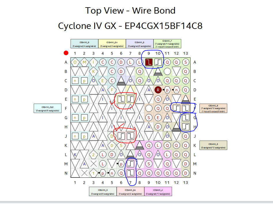
Image 1 : clock_pins_cycloneivgx
--------------------------------------------------------
Pin A9,A10 : clock
Pin F12,F13 : clock
pin G13,H13 : clock
pin E6,E7 : clock (transceiver 1 clock)
pin J6,J7 : clock (transceiver 0 clock)
pin M7,N7 : clock
Open up the attached reference manual and search for those pins. They all have some other functionality other than clock. What is going on here?!!?! the only thing that made sense was for J6,J7 where the document describes it as PCIE clock received from from the mother board...
Please help.
Link Copied
- Mark as New
- Bookmark
- Subscribe
- Mute
- Subscribe to RSS Feed
- Permalink
- Report Inappropriate Content
Hi,
As I understand it, you are observing some pin function mismatch between the pin planner vs the reference manual of the CIV GX starter devkit. From pin planner you are observing some pins as clock but in the manual, they have other functionality. Would you mind to help cross-checking with the devkit schematic on these pins to see if it matches the manual or pin planner.
Thank you very much.
Chee Pin
- Subscribe to RSS Feed
- Mark Topic as New
- Mark Topic as Read
- Float this Topic for Current User
- Bookmark
- Subscribe
- Printer Friendly Page