- Mark as New
- Bookmark
- Subscribe
- Mute
- Subscribe to RSS Feed
- Permalink
- Report Inappropriate Content
客户目前板子上做的 DDR4(SODIMM 72bit) ,当初做管脚验证的工程都可以编译通过,并且已经制版。
由于成本问题,客户想更换DDR4 厂家 ,接口还是SODIMM。现在修改了DDR4 IP (SODIMM 64bit) ,但是软件无法Fitter通过,请问这个无法Fitter 的原因是什么?
客户目前布局在 2k ,2l ,2m,2n 4个bank 里面,其中2l 是地址线,2k ,2m,2n 是数据线。
附件中我会把72bit 的工程,64bit 的工程上传给你,请协助分析一下,谢谢!
Link Copied
- Mark as New
- Bookmark
- Subscribe
- Mute
- Subscribe to RSS Feed
- Permalink
- Report Inappropriate Content
Hi,
Thank you for joining this Intel Community.
I am sorry but I didn't received any attachment as per mentioned. Can you help to re-attach so that I can take a closer look to your issue.
Thank you .
Regards,
Aida
- Mark as New
- Bookmark
- Subscribe
- Mute
- Subscribe to RSS Feed
- Permalink
- Report Inappropriate Content
- Mark as New
- Bookmark
- Subscribe
- Mute
- Subscribe to RSS Feed
- Permalink
- Report Inappropriate Content
- Mark as New
- Bookmark
- Subscribe
- Mute
- Subscribe to RSS Feed
- Permalink
- Report Inappropriate Content
Hi,
Thanks for sharing the designs. Please allow me sometime to look into the design. I shall come back to you with findings.
Thank you for your patience.
Regards,
Aida
- Mark as New
- Bookmark
- Subscribe
- Mute
- Subscribe to RSS Feed
- Permalink
- Report Inappropriate Content
Dear DXu2,
Please accept my apology for the delay in response due to public holiday in my region.
I've compiled your project and see the fitter error. Below is what I’ve been analyzed.
1) Top level file:
- I noticed that there is a mismatch between the DQ width in the top level file set in the project (s10_ddr4_top.v) and the DDR4 IP top level file (ddr_ip.v). I am not familiar on the modified top level file thus not able to edit it. Please help to change this accordingly. Refer below:
a) s10_ddr4_top.v = 72 bits --> inout wire [71:0] mem_dq,
b) ddr4_ip.v = 64bits --> inout wire [63:0] mem_dq
2) Assignment Editor:
- Pins is assigned for 72 bits data. Please remove extra 8 DQ data ( DQ [ 71:64]) in the QSF file and save.
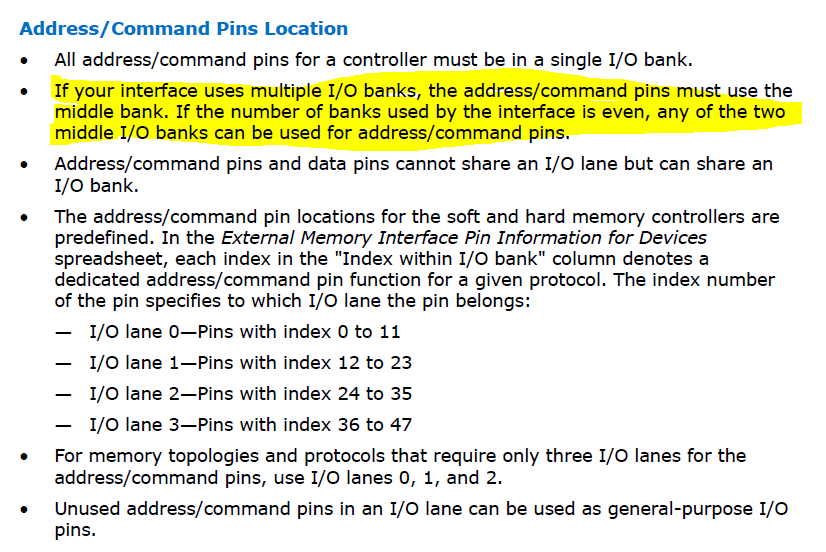
- Add/Cmd pins location: In the design, Add/Cmd pins were assigned to Bank 2L . The reason Fitter compilation failed is due to BANK 2L are not middle of IO bank where 64 bits DDR4 interface is placed. EMIF pin placement requirement required Address/Command/Control pin be placed in the middle of IO bank. This also mentioned in the Stratix 10 EMIF User guide.
Example as below.
- EMIF IO bank usage 3A, 3B, 3C : Address pin need to be in 3B
- EMIF IO bank usage 3B, 3C, 3D : Address pin need to be in 3C
- EMIF IO bank usage 2L, 2M, 2N : Address pin need to be in 2M
- Please change Add/Cmd pin to Bank 2M. To avoid any conflict or accidently placed the pins in wrong location, I suggest that you remove all the location assignment and only assign one DQ pin to Bank 2L ( for example : mem_dqs[0] to Bank 2L) and one Addr pins to Bank 2M ( for example: mem_a [0] to Bank 2M) and let Quartus auto-fit the rest of them.
It worked for me in a simplified example design test case project. Please try it for your your project pinout and let me know if it works OK. Hope this helps.😊
Thanks
Regards,
Aida
- Mark as New
- Bookmark
- Subscribe
- Mute
- Subscribe to RSS Feed
- Permalink
- Report Inappropriate Content
谢谢您的回复,
目前客户已经把板子做好了,当初他们管脚验证使用的72bit,目前想使用64bit 的,请问目前还有什么别的补救措施?
- Mark as New
- Bookmark
- Subscribe
- Mute
- Subscribe to RSS Feed
- Permalink
- Report Inappropriate Content
Dear DXu2,
I am sorry for the delay in response due to current workload.
Proper design practice is to verify fitter placement first before proceed to board design.
- If customer later decided to change EMIF design then I would expect customer to change their board design as well. As far as I'm aware of, there is no other option to this.
Normally it’s fine to reduce DQ width and by right it shouldn’t hit fitter error
- 72 bits = 64 bits + 8 ECC bits.
- Changing the design to 64 bits meaning customer just disable ECC option in EMIF IP so fitter should still work with x64 bit DQ
- Also, make sure that the add/cmd pins located at the middle bank as this is the requirement when using multiple I/O banks.
Sorry I couldn’t be more helpful. This is the best I can do. Let me know if there is any help needed.
Regards,
Aida
- Subscribe to RSS Feed
- Mark Topic as New
- Mark Topic as Read
- Float this Topic for Current User
- Bookmark
- Subscribe
- Printer Friendly Page
