- Mark as New
- Bookmark
- Subscribe
- Mute
- Subscribe to RSS Feed
- Permalink
- Report Inappropriate Content
MAX R 10 10M08 Eval Kit Board
Link Copied
- Mark as New
- Bookmark
- Subscribe
- Mute
- Subscribe to RSS Feed
- Permalink
- Report Inappropriate Content
Hi,
1.2 V volt is the the core voltage on MAX10 EVAL KIT.
What exactly you are trying to do explain with respect to the schematic please.
About which regulator you are talking about ? I can't tell exactly which features of max 10 will get impact if you change the voltages.
Check pin connection guiltiness.
However we can get required voltage (0.603V to VIN-0.5V) from regulator using external divider, check datasheet for the requirements.
Regards
Anand
- Mark as New
- Bookmark
- Subscribe
- Mute
- Subscribe to RSS Feed
- Permalink
- Report Inappropriate Content
Dear,
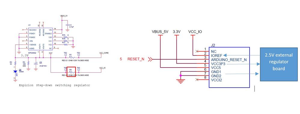
On the schematic of the Kit there are a regulator called U1(PN> EP5388QI), on this regulator is connected VCC_CORE and VCC_IO.
I need 2.5V on the VCCIOs but on this design of board there are just one regulator and if i change the voltage in this regulator(U1) the voltages of VCC_CORE and VCC_IO will be change together.
What You sugest to change the voltages on VCC_IO to 2.5V on this KIT?
Best regards,
Dan
- Mark as New
- Bookmark
- Subscribe
- Mute
- Subscribe to RSS Feed
- Permalink
- Report Inappropriate Content
Hi Dan,
Okay, It depends on Output voltage select pin 10,11,&12.
The regulator section board is designed by selecting one of seven preset output voltages here it is 3.3V, not by choose external divider.
I don't think we can change the voltage.
Regards
Anand
- Mark as New
- Bookmark
- Subscribe
- Mute
- Subscribe to RSS Feed
- Permalink
- Report Inappropriate Content
Dear,
I think the best way is disconnect the R4 Shunt resistor and supply the 2.5V using an external regulator connected in a J2 connector.
At least there are a possibility to use a external board. Thank you , if You have better suggestion , please, share.
Best regards,
Dan
- Mark as New
- Bookmark
- Subscribe
- Mute
- Subscribe to RSS Feed
- Permalink
- Report Inappropriate Content
Hi Dan,
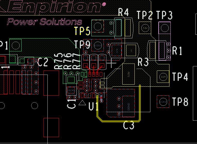
If we remove the R4 still, we will get 3.3V only.
Layout is designed like that. We don't have any via at R4.
Regards
Anand
- Mark as New
- Bookmark
- Subscribe
- Mute
- Subscribe to RSS Feed
- Permalink
- Report Inappropriate Content
Dear, The Idea is disconnect R4 and on TP5 side is connect the output from one external regulator with 2.5V, the bad side is to connect an external board with a regulator.
Best regards,
Dan
- Mark as New
- Bookmark
- Subscribe
- Mute
- Subscribe to RSS Feed
- Permalink
- Report Inappropriate Content

Its possible? The FPGA partnumber used on this board said that this is a Single Supply and can work with 3.3V on core and 2.5V on VCCIOs.
Best regards,
Daniel.
- Mark as New
- Bookmark
- Subscribe
- Mute
- Subscribe to RSS Feed
- Permalink
- Report Inappropriate Content
Hi Daniel,
Yes, We can remove the R4 and use J2.2 for external supply.
VCCIO is not monitored by POR so we can supply it any time we required. example : We can also power up VCCIO for IO banks individually after configuration based on our design requirements.
So, I am not seeing any problem, But however Intel will not be liable for any damage that you may occur as a result of modification, either with or without your knowledge.
Regards
Anand
- Mark as New
- Bookmark
- Subscribe
- Mute
- Subscribe to RSS Feed
- Permalink
- Report Inappropriate Content
Dear,
Thank You. Also, if You know another FPGA development Board that can support dual voltage supply let me know.
For the moment i will go with this solution.
Best regards,
Daniel.
- Mark as New
- Bookmark
- Subscribe
- Mute
- Subscribe to RSS Feed
- Permalink
- Report Inappropriate Content
Hi Daniel,
I can't find any FPGA development Board that can support dual voltage supply.
Regards
Anand
- Subscribe to RSS Feed
- Mark Topic as New
- Mark Topic as Read
- Float this Topic for Current User
- Bookmark
- Subscribe
- Printer Friendly Page
