- Mark as New
- Bookmark
- Subscribe
- Mute
- Subscribe to RSS Feed
- Permalink
- Report Inappropriate Content
Hi everyone,
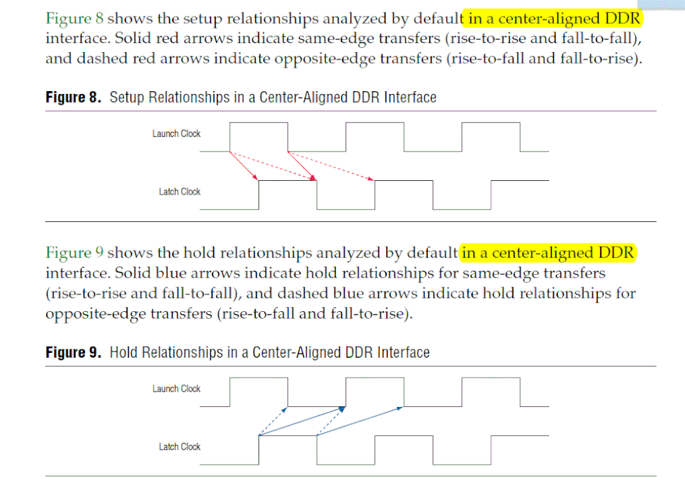
I don't know the thing in AN433, I feel it's wrong. Use the same edge to launch and latch data, How could two instructions appear?
Link Copied
- Mark as New
- Bookmark
- Subscribe
- Mute
- Subscribe to RSS Feed
- Permalink
- Report Inappropriate Content
- Mark as New
- Bookmark
- Subscribe
- Mute
- Subscribe to RSS Feed
- Permalink
- Report Inappropriate Content
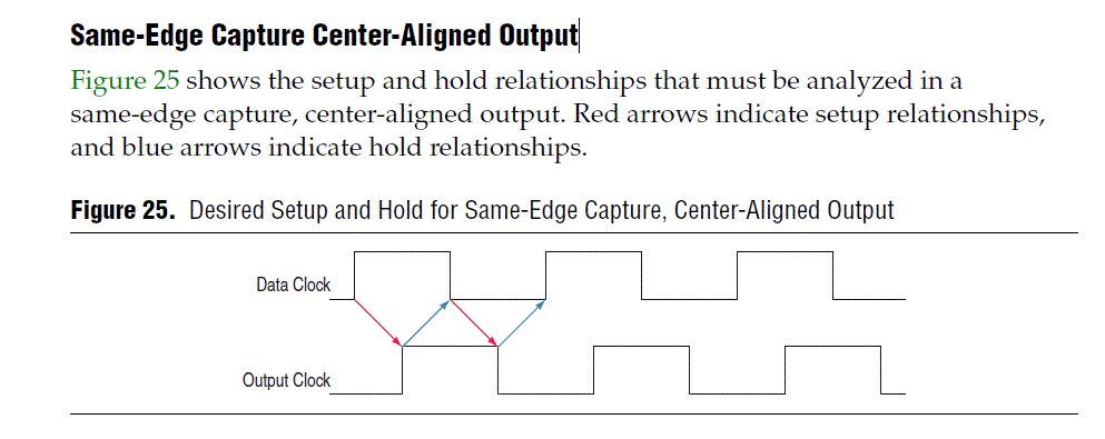
No, the diagrams are correct. For same edge capture, you perform same edge setup analysis and opposite edge hold analysis. Figure 9 is not very useful since it's just showing what all the relationships look like. Figure 25 is what should be used. I also prefer the online training to this document. See it here: https://www.intel.com/content/www/us/en/programmable/support/training/course/oddr1000.html
#iwork4intel
- Mark as New
- Bookmark
- Subscribe
- Mute
- Subscribe to RSS Feed
- Permalink
- Report Inappropriate Content
Hi sstrell,
I have one problem about the centric-alignment DDR source synchronization input , if upstream device provide the requirement the setup and holdup information of FPGA, It means that if the trace delay of data and clk on the PCB is equal, upstream device can ensure that the data and clk is centric-alignment at the input port of FPGA, and I calculate the man and min input delay which is the trace delay limitation between data and clk in FPGA (like below figure)? Another question, if the phase relationship between data and output clk of upstream device, is necessray for me to set constrains for source synchronization input ?
Best regrads,
Lambert
- Mark as New
- Bookmark
- Subscribe
- Mute
- Subscribe to RSS Feed
- Permalink
- Report Inappropriate Content
Yes, Figure 25 better illustrate the setup and hold requirement for the data latching.
- Mark as New
- Bookmark
- Subscribe
- Mute
- Subscribe to RSS Feed
- Permalink
- Report Inappropriate Content
Hi BCT_Intel
I am leaning the source synchronization constrains, but I am confused about centric-FPGA method just because that there is no complete diagram to illustrate the relationship about vritual clk, input/output clk and data input/output liking internal reg-to-reg. And I don't know how the quartus II to complete route based on the information. Can you provide me some help about this? I have watch the training class, I can't complete understand this method.
Best regards,
Lambert
- Mark as New
- Bookmark
- Subscribe
- Mute
- Subscribe to RSS Feed
- Permalink
- Report Inappropriate Content
Hello sir,
Basically the AN433 describe it clearly, especially page 18. If needed, you can specific which part that you are not understand here and see if we can help to clarify.
By the way, maybe this link also helpful for you - https://www.intel.com/content/www/us/en/programmable/support/support-resources/design-examples/design-software/timinganalyzer/exm-tq-ca_ss_in.html
- Subscribe to RSS Feed
- Mark Topic as New
- Mark Topic as Read
- Float this Topic for Current User
- Bookmark
- Subscribe
- Printer Friendly Page


