- Mark as New
- Bookmark
- Subscribe
- Mute
- Subscribe to RSS Feed
- Permalink
- Report Inappropriate Content
Good morning,
I require assistance to understand the difference in the architecture between two batched of the same product, namely EPM240T100I5N.
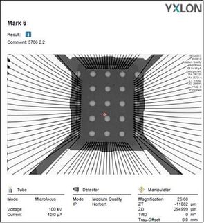
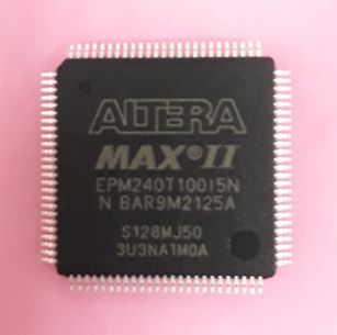
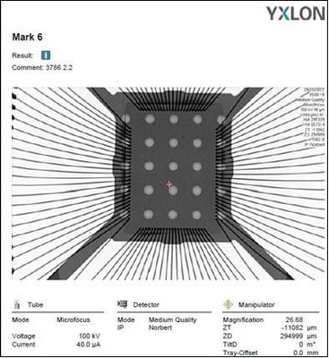
The pictures below show the x-ray image & its corresponding marking the of batch with "holes":
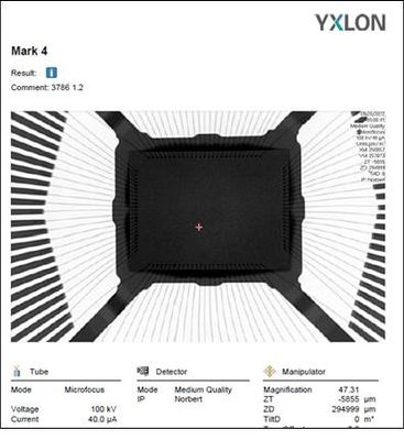
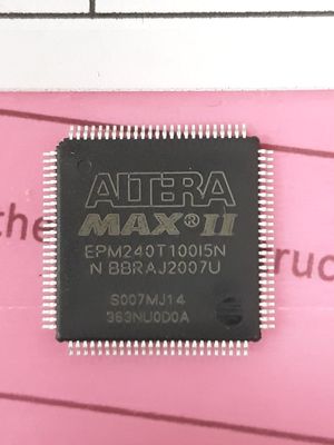
The following pictures, similarly show the x-ray image & its corresponding marking the of batch with " NO holes":
Our difficulty lays in understanding the difference between the two product architectures, the reason for the "holes" in the first batch and why they are not present in the second batch with "NO holes".
Please evaluate my query and kindly let me know your clarifications for this case.
Kind regards
Alex Bonello
Purchasing Executive
Bavarian Technology Systems
F16-F18 Tübingen Centre
Mosta Technopark
Mosta MST3000
Malta
Tel: +356 23399109
Fax: +356 21422227
Email: alex.bonello@btsmalta.com
- Mark as New
- Bookmark
- Subscribe
- Mute
- Subscribe to RSS Feed
- Permalink
- Report Inappropriate Content
Hi BtsMalta2022,
Just got feedback from the internal. Both designs are normal. The “holes” below are not holes, but dimples on bottom of die pad. It is to enhance mold to die pad adhesion. This is a newer design.
Regards,
Fakhrul
Link Copied
- Mark as New
- Bookmark
- Subscribe
- Mute
- Subscribe to RSS Feed
- Permalink
- Report Inappropriate Content
Hi BtsMalta2022,
I need to clarify it internally first and will get back to you.
Regards,
Fakhrul
- Mark as New
- Bookmark
- Subscribe
- Mute
- Subscribe to RSS Feed
- Permalink
- Report Inappropriate Content
Hi Fakhrul,
Thank you for following up to my post.
Any updates, please?
Also, may I know your technical position at Intel, please?
Kind regards
Alex Bonello
Purchasing Executive
Bavarian Technology Systems
F16-F18 Tübingen Centre
Mosta Technopark
Mosta MST3000
Malta
Tel: +356 23399109
Fax: +356 21422227
Email: alex.bonello@btsmalta.com
- Mark as New
- Bookmark
- Subscribe
- Mute
- Subscribe to RSS Feed
- Permalink
- Report Inappropriate Content
Hi BtsMalta2022,
I'm an Application engineer. I have escalated your issue and currently, this issue has been directed to the Packaging R&D Engineering team. It may take a while to get their feedback. I will plan on letting you know as soon as I learn more information.
Regards,
Fakhrul
- Mark as New
- Bookmark
- Subscribe
- Mute
- Subscribe to RSS Feed
- Permalink
- Report Inappropriate Content
Hi BtsMalta2022,
Just want to update you that I am still pending the answer from the internal team.
I shall come back to you with the findings.
Regards,
Fakhrul
- Mark as New
- Bookmark
- Subscribe
- Mute
- Subscribe to RSS Feed
- Permalink
- Report Inappropriate Content
Hi BtsMalta2022,
We are pending for a response from subcon. Will get back to you by today or tmr.
BTW, on the 2nd x-ray photo, the x-ray image seems too dark. Can you lower the contrast so that it looks the same as 1st x-ray photo?
Regards,
Fakhrul
- Mark as New
- Bookmark
- Subscribe
- Mute
- Subscribe to RSS Feed
- Permalink
- Report Inappropriate Content
Hi Fakhrul,
Thank you for your feedback.
Will forward your suggestion to management and return asap,
In the meantime, looking forward to your team's conclusions.
Regards
Alex
- Mark as New
- Bookmark
- Subscribe
- Mute
- Subscribe to RSS Feed
- Permalink
- Report Inappropriate Content
Hi Alex,
We are still pending for the information. Meanwhile do share us if you have any finding on the latest inquiry.
Regards,
Bruce
- Mark as New
- Bookmark
- Subscribe
- Mute
- Subscribe to RSS Feed
- Permalink
- Report Inappropriate Content
Hi BtsMalta2022,
Just got feedback from the internal. Both designs are normal. The “holes” below are not holes, but dimples on bottom of die pad. It is to enhance mold to die pad adhesion. This is a newer design.
Regards,
Fakhrul
- Subscribe to RSS Feed
- Mark Topic as New
- Mark Topic as Read
- Float this Topic for Current User
- Bookmark
- Subscribe
- Printer Friendly Page
