- Mark as New
- Bookmark
- Subscribe
- Mute
- Subscribe to RSS Feed
- Permalink
- Report Inappropriate Content
I'm writing an project to access system ddr4 (read & write). In Quartus Pro 19.2 Platform designer, I added "EMIF IP" inside, and add a top.v as well.
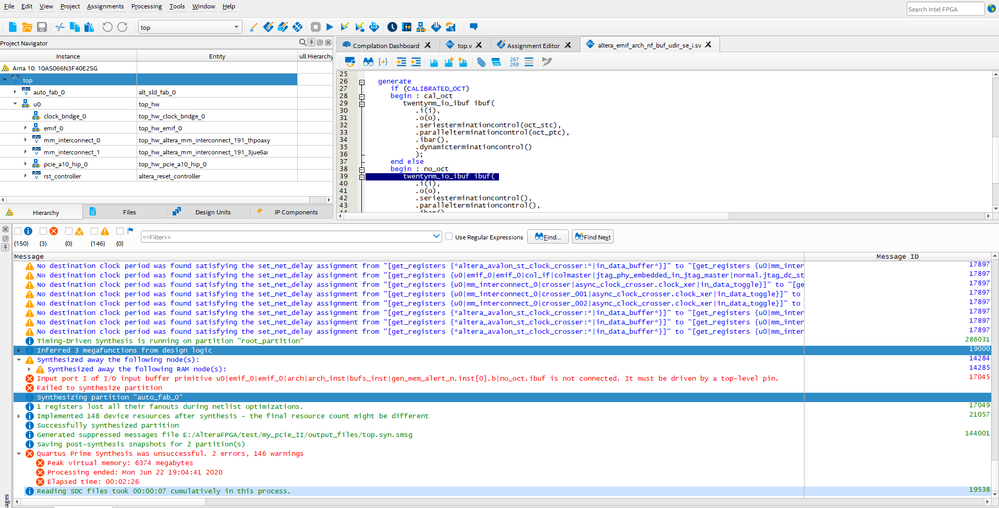
But when trying to compile, it reports some err message as following:
"Error (17045): Input port I of I/O input buffer primitive u0|emif_0|emif_0|arch|arch_inst|bufs_inst|gen_mem_alert_n.inst[0].b|no_oct.ibuf is not connected. It must be driven by a top-level pin. File: E:/AlteraFPGA/test/my_pcie_II/platform/top_hw/ip/top_hw/top_hw_emif_0/altera_emif_arch_nf_191/synth/altera_emif_arch_nf_buf_udir_se_i.sv Line: 39
Error: Failed to synthesize partition
Info: Synthesizing partition "auto_fab_0"
.."
What does this error mean ? And HOW to fix it ? thanks ~
Link Copied
- Mark as New
- Bookmark
- Subscribe
- Mute
- Subscribe to RSS Feed
- Permalink
- Report Inappropriate Content
continue ..
in << External Memory Interface Handbook Volume 2: DesignGuidelines。pdf >>
- 7.4.3.2. Arria 10 EMIF IP DDR4 Parameters: Memory
there mentions as below: " Enable ALERT#/PAR pins - MEM_DDR4_ALERT_PAR_EN " which describes as following- " .. Allows address/command calibration, which may provide better margins on the address/command bus. .
The parity pin is a dedicated pin in the address/command bank, but the alert_n pin can be placed in any bank that spans the memory interface. You should explicitly choose the location of the alert_n pin and place it in the address/command bank.
"
Could I disable this " Enable ALERT#/PAR pins " in Arria 10 SOC ? If it's mandatory pin, how should I assign pin for it (alert_n) ? Thanks great for any help.
/jet
- Mark as New
- Bookmark
- Subscribe
- Mute
- Subscribe to RSS Feed
- Permalink
- Report Inappropriate Content
By right you will see a RZQ pin in the IP top level file. You need to export this pon to top level and assign with an input pin.
- Subscribe to RSS Feed
- Mark Topic as New
- Mark Topic as Read
- Float this Topic for Current User
- Bookmark
- Subscribe
- Printer Friendly Page
