- Mark as New
- Bookmark
- Subscribe
- Mute
- Subscribe to RSS Feed
- Permalink
- Report Inappropriate Content
Hi all,
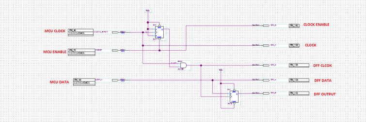
I starting with vhdl, and build this first design,
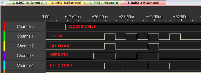
Than I wrote to a cyclone II device and got this:
From this circuit, I was expecting that dff output goes high at DFF clock rising edge and stay high. But it goes low at clock rising edge even that clock signal doesn't feeds dff directly.
Could someone help with this? Any help apreciated.
- Mark as New
- Bookmark
- Subscribe
- Mute
- Subscribe to RSS Feed
- Permalink
- Report Inappropriate Content
Hi,
I tried to simulate the design; there is a spike in the DFF_Clock that causes the output of signal DFF_output as shown in waveform.PNG.
You may consider to remove the JK FF and AND gate.
Thanks.
Best regards,
KhaiY
Link Copied
- Mark as New
- Bookmark
- Subscribe
- Mute
- Subscribe to RSS Feed
- Permalink
- Report Inappropriate Content
Hi,
Could you share the design for investigation?What is the software edition/version you are using?
Thanks.
Best regards,
KhaiY
- Mark as New
- Bookmark
- Subscribe
- Mute
- Subscribe to RSS Feed
- Permalink
- Report Inappropriate Content
My software is:
and attached, my design.
- Mark as New
- Bookmark
- Subscribe
- Mute
- Subscribe to RSS Feed
- Permalink
- Report Inappropriate Content
- Mark as New
- Bookmark
- Subscribe
- Mute
- Subscribe to RSS Feed
- Permalink
- Report Inappropriate Content
Hi KhaiY,
I've changed my design, excluding AND gate and and some other changes and it worked,
thanks for your time and efforts
Mentz
- Mark as New
- Bookmark
- Subscribe
- Mute
- Subscribe to RSS Feed
- Permalink
- Report Inappropriate Content
Hi,
I’m glad that your question has been addressed, I now transition this thread to community support. If you have a new question, feel free to open a new thread to get the support from Intel experts. Otherwise, the community users will continue to help you on this thread. Thank you.
Best regards,
KhaiY
- Subscribe to RSS Feed
- Mark Topic as New
- Mark Topic as Read
- Float this Topic for Current User
- Bookmark
- Subscribe
- Printer Friendly Page


