- Mark as New
- Bookmark
- Subscribe
- Mute
- Subscribe to RSS Feed
- Permalink
- Report Inappropriate Content
We are using 2 Max 5 devices in our board, identical part numbers 5M2210ZF324 with similar board designs for each device. While we are able to program one of the devices successfully, we are getting a verification failure when attempting to program the second device. Erase operation is successful.. Blank check, program/configure and verify operations are all failing. We have also replaced the second device suspecting CPLD. However, issue persists with replaced part also.
Link Copied
- Mark as New
- Bookmark
- Subscribe
- Mute
- Subscribe to RSS Feed
- Permalink
- Report Inappropriate Content
Do you have two devices in one JTAG chain? Or two separate chains?
Signal integrity can be an issue. JTAG can be fussy. Do you have any long, unbuffered traces?
Cross talk - do you have any nearby signals causing interference?
Cheers,
Alex
- Mark as New
- Bookmark
- Subscribe
- Mute
- Subscribe to RSS Feed
- Permalink
- Report Inappropriate Content
Thank you for your reply a_x_h_75.
Do you have two devices in one JTAG chain? Or two separate chains? - We have separate JTAG chains.
Do you have any long, unbuffered traces? - We do have long traces, but as cross-verified against the Max 5 development board, the trace lengths of TCK, TMS, TDI and TDO on our board are lesser than the trace lengths of the development board (about 3000 mils). Our longest trace length is about 2850 mils. We have also ensured the recommended terminations (TCK pull-down to GND with 1k ohm, TDI and TMS pull-up to VCCIO1 with 10k ohm each, TDO floating, DEV_OE and DEV_CLRn unused and tied to GND).
One more point of relevance is that during board fab, the connections from CPLD to JTAG header got mixed up (in the JTAG chains of both devices) - CPLD TMS routed to Header TDO, CPLD TDI routed to Header TCK, CPLD TCK routed to Header TDI and CPLD TDO to Header TMS. As a result, we were forced to make a tiny mating adapter with the JTAG Header to switch the signals correctly. The USB Blaster is connected to this adapter now. This arrangement is temporarily OK since it works with the first device. During our experiments, we have now routed the JTAG signals directly from the CPLD BGA pins (along with termination resistors) to an alternate JTAG header. This was to ensure the reduced trace lengths for the non-working device. But still, no luck.
Do you have any nearby signals causing interference? - There are devices like NVRAM, voltage level translators, opto-isolators nearby. But the working device also has the same kind of devices nearby. Anyhow, we have monitored the VCCIO1, GND, TMS, TCK, TDI and TDO signals during a Program operation and not found any abnormal electrical behavior. Plus, both CPLDs do get detected by the USB Blaster (Device ID & silicon ID read with Auto-detect operation).
- Mark as New
- Bookmark
- Subscribe
- Mute
- Subscribe to RSS Feed
- Permalink
- Report Inappropriate Content
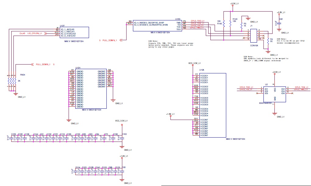
Please find attached, JTAG-related schematic screenshot for reference.
Additional info:
We are using Quartus Prime Version 18.1.0 Build 625 09/12/2018 SJ Standard Edition.
System Configuration is:
Windows Edition: Windows 10 Enterprise
Processor: Intel Core i5-4590 CPU @ 3.30 GHz
RAM: 12.0 GB
System Type: 64-bit OS, x64-based processor
- Mark as New
- Bookmark
- Subscribe
- Mute
- Subscribe to RSS Feed
- Permalink
- Report Inappropriate Content
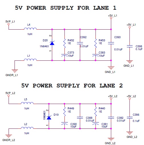
Update:
We have tried to use the power rail (5V with filter network) of working device to power up and program the non-working CPLD (after isolating the existing power rail to non-working CPLD). And we are seeing that the Program/Configure and Blank-check operations are now intermittently successful (say out of 10 attempts, at least 5 - 6 times successful). The filtering of 5V is attached in the screenshot.
- Mark as New
- Bookmark
- Subscribe
- Mute
- Subscribe to RSS Feed
- Permalink
- Report Inappropriate Content
This is all pointing at a signal integrity issue. Whilst the trace lengths you specified aren't a problem I'm concerned that the adaptor you had to make is contributing to the problem.
Can you make an active adaptor board? Buffer the signals from the Blaster onto the target. That'll help. Buffer TDO back to the Blaster as well.
Are you using a genuine USB-Blaster?
Cheers,
Alex
- Mark as New
- Bookmark
- Subscribe
- Mute
- Subscribe to RSS Feed
- Permalink
- Report Inappropriate Content
Thank you for the suggestion a_x_h_75 and apologies for the late update. We have requested a signal and power integrity analysis for the jtag and surrounding circuitry. Should get that in a couple of days. However, we no longer suspect insufficient buffering of JTAG lines as an issue.
Based on our experiments, we have strong reason to believe that the input power supply filtering and voltage regulation from 5 V to 1.8 V may be the culprit. The non-working CPLD power supply path shows a 6KHz frequency variation on the 1.8 V regulated output (almost 500 mV - 1.7 V to 2.2 V). Same signal on another working board shows only 1.8 V varying from 1.7 V to 1.9 V (200 to 250 mV).
We also saw that using the 3.3 V to generate the 1.8 V supply resulted in a noise variation of 200 to 250 mV on 1.8 V line. And significantly, we were able to program the non-working device through same JTAG setup successfully and consistently (30 out of 30 times).
I am sure that our USB Blaster is genuine. We ordered it from an authorized vendor (Mouser or Digikey). Is there any other way to verify the genuineness of the Blaster?
- Mark as New
- Bookmark
- Subscribe
- Mute
- Subscribe to RSS Feed
- Permalink
- Report Inappropriate Content
I've never seen a third party Blaster that actually looks like the original; all the ones I've seen a branded differently. So, if yours looks like the real thing it probably is.
It should certainly have a flexible PCB cable that connects to your target.
Cheers,
Alex
- Subscribe to RSS Feed
- Mark Topic as New
- Mark Topic as Read
- Float this Topic for Current User
- Bookmark
- Subscribe
- Printer Friendly Page