- Mark as New
- Bookmark
- Subscribe
- Mute
- Subscribe to RSS Feed
- Permalink
- Report Inappropriate Content

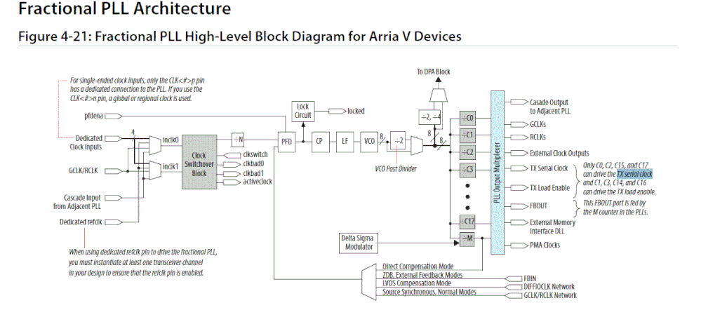
I have one problem is that I need several LVDS pairs for high-speed data output, I only can select the lvds pairs in diffent bank because of layout restrictions. I chose the output of one external PLL to drive them, but it always was fittered failure, I read the clock , PLL and I/0 part of Arria V datasheet, it can't say that the same external PLL can not drive lvds pairs in different BANK obviously. I want to know what kind of routing resources (GCLK, RCLK or PCLK) the arriav_pll_lvds_output of the PLL chooses.
Can you give me some help?
Thank,
Lambert
Link Copied
0 Replies
Reply
Topic Options
- Subscribe to RSS Feed
- Mark Topic as New
- Mark Topic as Read
- Float this Topic for Current User
- Bookmark
- Subscribe
- Printer Friendly Page