Board Skew Parameter Tool Guide
Success! Subscription added.
Success! Subscription removed.
Sorry, you must verify to complete this action. Please click the verification link in your email. You may re-send via your profile.
- Intel Community
- Intel Community Knowledge Base
- Product Support Forums Knowledge Base
- FPGA Knowledge Base
- FPGA Wiki
- Board Skew Parameter Tool Guide
Board Skew Parameter Tool Guide
- Subscribe to RSS Feed
- Mark as New
- Mark as Read
- Bookmark
- Subscribe
- Printer Friendly Page
- Report Inappropriate Content
Board Skew Parameter Tool Guide
version v16.0
This tool is targeted to be used in Microsoft Excel 2010. You may face compatibility issues with earlier versions of Excel.
PCB traces can have skews between them which can cause timing margins to be reduced. Further, margin reduction can occur due to skews between different ranks in multi-rank topologies. With the increase in operating frequencies for memory interfaces, it has become increasingly important to enter accurate Board Skew Parameters for the External Memory Interfaces IP during the IP Catalog flow. This tool will enable you to calculate these board skew parameters faster and more easily. You can calculate these parameters by selecting your memory interface configuration and then entering in simulated trace delays for memory interface traces. For "How to Simulate", please refer to this FPGA wiki article: Arria 10 EMIF Simulation Guidance
The tool workbook has been divided into 5 sheets:
1. Introduction:
This page acts as the 'Home' Page for the Tool
- Enter: This allows you to proceed into the Tool
- Handbook: This button is a link to the Altera EMIF Handbook where you can find all the Board Skew Parameter definitions and additional information. The latest information will be available in version Handbook version 16.1
- Guide: This button directs you to this page to guide you through the rest of the tool
2. Interface IP:
Choose either the Arria 10 IP button for Arria 10 External Memory Interfaces IP or UniPHY IP button for UniPHY External Memory Interfaces IP depending on the interface you have chosen in the Altera IP Catalog.
3. Choose Protocol:
Choose the protocol you want to calculate board skew parameters for (should match the protocol chosen in the Altera IP Catalog
- Arria 10 External Memory Interfaces
DDR3, DDR4, QDRII/II+/II+Xtreme, QDR4 ,RLDRAM3
- UniPHY External Memory Interfaces
DDR2, DDR3, LPDDR2, QDRII/II+/II+Xtreme, RLDRAM 2&3
2/2f/IP_parameter_screen_capture.JPG
Fig-1: Arria10 DRR4 EMIF Protocol BSPT IP Parameter pop-up Window.
Users will choose their configuration in the pop-up toolbox window
4. Spreadsheet:
Enter your simulated trace delays and package delays into the tables
- Export: To save data entered in by the user on the 'Spreadsheet' sheet, click on the Export button. This will allow you to copy and paste the data back into this sheet if necessary.
- Calculate: this button calculates the board skews based on the input trace and package delays you have provided and results are displayed in the ‘skew calculation’ sheet
Important Note:
i. Blank spaces do not equal 0.
ii. Please enter a value between the maximum and minimum table delays for all unused blank spaces. For Example. If there are 3 CK trace delay cells and you only want to use 2, choose one of the actual trace delay values from the two cells and copy it into the 3rd cell. The tool will use 0 as the minimum trace delay if left blank which will lead to wrong Board Skew Parameter calculations
iii. Enter delays inside the whitespaces only. If users modify any non-white areas, the tool may calculate inaccurate board skews
iv. Enter in package delays for traces you plan to deskew with board traces (The tool will calculate the total delay for you)
5. Skew Calculation:
This sheet holds the calculated skew which needs to be entered into the External Memory Interface IP parameter's board skew tab. It is highly recommended to use this calculated delay for IP generation to get accurate timing closure.
- To save Board Skew Parameters generated by the tool on the 'Skew Calculations' sheet, click on the Export button. It is recommended that you do so, to avoid loss of data entered into BSPT after saving and closing the excel tool.
- This will allow you to save a copy of the results in the Board Skew Parameter Tool. Please rename these exported sheets in excel to minimize confusion.
Important Note:
For re-calculation, please restart the entire process by going back to the first sheet(Introduction Sheet) using the back button. Doing so will reset all global variable assignments to initial values and avoid any incorrect calculation which occurs due to the use of global variables with non-initial values.
Frequently asked questions (FAQs):
Q. When should I use this tool?
Ans: This tool should be used during memory IP generation in IP Catalog to enter accurate Board Skew Parameter Values calculated from the user's PCB delay. The tool calculates these Board Skew Parameters accurately and displays it to you on the "Skew Calculations" Page. These parameters are entered under the Board Timing Tab > Board and Package Skew in the IP Catalog GUI.
Q. How accurate is this tool?
Ans: The tool calculates board skew parameters according to Altera's recommended formula best suited for using our FPGA products.
Q. Where can I download this tool or check for newer versions?
Ans: The tool can be found under Board Skew Parameter Tool (XLS) on Altera's External Memory Interface Solutions Center:
https://cdrdv2.intel.com/v1/dl/getcontent/652693
OR
Download using the link at the bottom of this wiki page
Please keep checking the above link for newer versions or any updates made to the tool
Q. Why there is no support for LPDDR3?
Ans: For LPDDR3, you can use DDR3 calculation support, as the underlying skew calculation equations are the same.
Measuring Delay Values:
Please follow the Altera EMIF Handbook when measuring delays (Page 92)
Non-fly-by topology (Balanced Tree)
- For discrete devices–all the delay (CK, Addr/Cmd, DQ, and DQS) from the FPGA are right to every memory device
- For UDIMMs–all the delays (CK, Addr/Cmd, DQ, and DQS) from the FPGA to the UDIMM connector for every memory device on the UDIMM. If UDIMM delay information is available, calculate delays to every memory device on the UDIMM.
- For RDIMMs–the Addr/Cmd and CK delay are from the FPGA to the register on the RDIMM. The DQ and DQS delay is from FPGA to RDIMM connectors for every memory device on the RDIMM.
- For LRDIMMS–the delay from the FPGA to the register on the LRDIMM.
Fly-by topology
- For discrete devices–the Addr/Cmd and CK delay are from the FPGA to the first memory device. The DQ and DQS delay is from FPGA to every memory device.
- For UDIMMs–the Addr/Cmd and CK delay are from the FPGA to the UDIMM connector for the first memory device on the UDIMM. The DQ and DQS delay is from the FPGA to UDIMM connector for every memory device on the UDIMM.
- For RDIMMs–the Addr/Cmd and CK delay are from the FPGA to the register on the RDIMM. The DQ and DQS delay is from FPGA to RDIMM connectors for every memory device on the RDIMM.
- Most DIMM types have signal group trace delays matched on the DIMM. Note that some multiple rank DIMMs have different propagation delays for the address/command and the control signals which leads to higher skews. It is recommended that users perform multi-board simulations to verify the signal propagation delays.
- For LRDIMMS–the delay from the FPGA to the buffer on the LRDIMM.
Non Supported topologies
- For memory topologies unsupported by this tool, users may calculate board skew parameters for each memory device and take the worst-case value for each board skew parameter across all the memory devices.
- Example: Mixed width device Interface. The 40-bit interface is made up of two 16bit devices and one 8bit device. You would treat each 16bit device as an interface and generate two board skew parameter tables in the 'Skew Calculations' sheet. You would then generate a board skew parameter table treating the 8bit device as a separate interface. When generating your memory interface using IP Catalog or Megawizard take the worst-case board skew value across all three tables for each Board Skew Parameter.
For multiple DDR discrete components/devices
- This tool can calculate board skew for up to 9 discrete devices provided the memory device widths are the same across all devices.
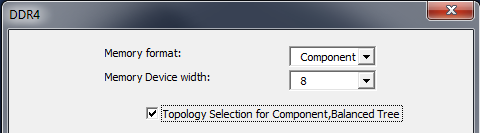
- If your interface is using discrete DDR2/3 devices, and the "balanced tree" option is selected, you will also unlock the ability to choose the 'Memory Device width'. The memory device widths allowed are 4, 8, and 16. This tool assumes the Memory Device width is the same across all the devices.
- 1/19/Capture_Balancedtree.PNG
Fig-2: Arria10 DRR4 EMIF Protocol pop-up Window 'Memory Device Width' Option.
- As an example, if your total interface width is 80 bits wide and your memory device width is 16 bits wide. Each device has two DQS groups(Device 0 has DQS groups 0 and 1, Device 1 has DQS groups 2 and 3, etc). Then the tool assumes the memory interface has 5 discrete devices and will provide enough cells to input trace delays going from the Altera FPGA to each of the 5 devices. The propagation delays entered for each memory device are measured from the FPGA to each memory device(for a balanced tree).
Not supported BSPT Component Memory format configuration
The current version of the BSPT will not support the following configuration with components
- Two-chip select with NO Clamshell board layout.
Selecting the option of clamshell or no clamshell during the IP configuration pop-up window in BSPT, will not have any impact. This selection was created specifically for No clamshell configuration.
Download Tool
Community support is provided during standard business hours (Monday to Friday 7AM - 5PM PST). Other contact methods are available here.
Intel does not verify all solutions, including but not limited to any file transfers that may appear in this community. Accordingly, Intel disclaims all express and implied warranties, including without limitation, the implied warranties of merchantability, fitness for a particular purpose, and non-infringement, as well as any warranty arising from course of performance, course of dealing, or usage in trade.
For more complete information about compiler optimizations, see our Optimization Notice.