CPRI IP v6 Latency Formula & Calculation Example
Success! Subscription added.
Success! Subscription removed.
Sorry, you must verify to complete this action. Please click the verification link in your email. You may re-send via your profile.
- Intel Community
- Intel Community Knowledge Base
- Product Support Forums Knowledge Base
- FPGA Knowledge Base
- FPGA Wiki
- CPRI IP v6 Latency Formula & Calculation Example
CPRI IP v6 Latency Formula & Calculation Example
- Subscribe to RSS Feed
- Mark as New
- Mark as Read
- Bookmark
- Subscribe
- Printer Friendly Page
- Report Inappropriate Content
CPRI IP v6 Latency Formula & Calculation Example
Updated on 20 July, 2016
Introduction
This page provides the following information to help the to understand and calculate their total delay budget of the em with CPRI IP v6:
- Fixed latency values of different sub-components within CPRI v6 IP
- Fixed latency values of other collateral products (IQ Mapper/DeMapper, Compression blocks) of CPRI v6 solutions
- How-to use the measurement features
- How-to use the calibration features
- Examples of calculating the total delay budget of CPRI IP v6 solution
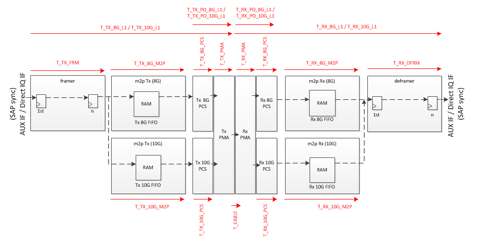
L1 Latency
Figure 1: Components of entire L1 and Latency Term Definition
Table 1: Latency Components and its definition
| L1 Part | Description | Latency Component | Sub Components |
|---|---|---|---|
| 8b10b variants | For 614.4, 1228.8, 2457.6, 3072, 4916.2, 6144 and 9830.4 Mbps | ||
| Full Tx | Full Transmitter path | T_TX_8G_L1 | T_TX_MO_8G_L1 + T_TX_PO_8G_L1 |
| PHY Tx | Physical only Transmitter path | T_TX_PO_8G_L1 | T_TX_8G_PCS + T_TX_PMA |
| MAC Tx | MAC Only Transmitter path | T_TX_MO_8G_L1 | T_TX_FRM + T_TX_8G_M2P |
| Full Rx | Full Receiver path | T_RX_8G_L1 | T_RX_PO_8G_L1 + T_RX_MO_8G_L1 |
| PHY Rx | Physical only Receiver path | T_RX_PO_8G_L1 | T_RX_PMA + T_RX_8G_PCS |
| MAC Rx | MAC only Receiver path | T_RX_MO_8G_L1 | T_RX_8G_M2P + T_RX_DFRM |
| 64/66b variants | For 8110.08, 10137.6 and 12165.12 Mbps | ||
| Full Tx | Full Transmitter path | T_TX_10G_L1 | T_TX_MO_10G_L1 + T_TX_PO_10G_L1 |
| PHY Tx | Physical only Transmitter path | T_TX_PO_10G_L1 | T_TX_10G_PCS + T_TX_PMA |
| MAC Tx | MAC Only Transmitter path | T_TX_MO_10G_L1 | T_TX_FRM + T_TX_10G_M2P |
| Full Rx | Full L1 Receiver path | T_RX_10G_L1 | T_RX_PO_10G_L1 + T_RX_MO_10G_L1 |
| PHY Rx | Physical only Receiver path | T_RX_PO_10G_L1 | T_RX_PMA + T_RX_10G_PCS |
| MAC Rx | MAC only Receiver path | T_RX_MO_10G_L1 | T_RX_10G_M2P + T_RX_DFRM |
Table 2: Sub-component Latency Value according to device family and line bit rate
| Latency Component | Device | Line bit rate (Mbps) | Core clock | PCS clock | UI | Remarks |
|---|---|---|---|---|---|---|
| T_TX_FRM | All | All | 4 | - | 160 | |
| T_TX_8G_M2P | All | 614.4 | tx_8g_ex_delay + 0.5 | - | (tx_8g_ex_delay x 40) + 20 | |
| All | 1228.8 - 9830.4 | tx_8g_ex_delay + 2 | - | (tx_8g_ex_delay x 40) + 80 | ||
| T_TX_10G_M2P | All | 8110.08, 10137.6, 12165.12 | tx_10g_ex_delay + 3 | - | (tx_10g_ex_delay x 40) + 120 | |
| T_TX_8G_PCS | Gen V | 614.4 | 0.75 | - | 30 | Assume Tx bitslip (register XCVR_BITSLIP) is not used |
| 1228.8 - 9830.4 | 2 | - | 80 | Assume Tx bitslip (register XCVR_BITSLIP) is not used | ||
| Arria 10 | 614.4 | 0.75 | - | 30 | Assume Tx bitslip (register XCVR_BITSLIP) is not used | |
| 1228.8 - 9830.4 | 2 | - | 80 | Assume Tx bitslip (register XCVR_BITSLIP) is not used | ||
| T_TX_10G_PCS | Gen V | 8110.08, 10137.6, 12165.12 | - | 6.8 | 272 | Assume Tx bitslip (register XCVR_BITSLIP) is not used |
| Arria 10 | - | 6.8 | 272 | Assume Tx bitslip (register XCVR_BITSLIP) is not used | ||
| T_TX_PMA | Gen V | 614.4 | 1.325 | - | 53 | |
| 1228.8 - 9830.4 | 2.075 | - | 83 | |||
| 8110.08, 10137.6, 12165.12 | - | 3.075 | 123 | |||
| Arria 10 | 614.4 | 1.075 | - | 43 | ||
| 1228.8 - 9830.4 | 1.975 | - | 79 | |||
| 8110.08, 10137.6, 12165.12 | - | 3.675 | 147 | |||
| T_CABLE | Please refer to the medium
specification |
|||||
| T_RX_PMA | Gen V | 614.4 | 0.65 | - | 26 | Assume XCVR_BITSLIP is not used |
| 1228.8 - 9830.4 | 0.775 | - | 31 | |||
| 8110.08, 10137.6, 12165.12 | - | 1.525 | 61 | |||
| Arria 10 | 614.4 | 0.6125 | - | 24.5 | ||
| 1228.8 - 9830.4 | 1.0125 | - | 40.5 | |||
| 8110.08, 10137.6, 12165.12 | - | 1.6625 | 66.5 | |||
| T_RX_8G_PCS | Gen V | 614.4 | 2 | - | 80 | |
| 1228.8 - 9830.4 | 5.5 or 6* | - | 220 or 240* | |||
| Arria 10 | 614.4 | 1.5 | - | 60 | ||
| 1228.8 - 9830.4 | 9 | - | 360 | |||
| T_RX_10G_PCS | Gen V | 8110.08, 10137.6, 12165.12 | - | 7.125 | 285 | |
| Arria 10 | 8110.08, 10137.6, 12165.12 | - | 7.125 | 285 | ||
| T_RX_8G_M2P | All | 1228.8 - 9830.4 | rx_8g_ex_delay + 5 | - | (rx_ex_delay x 40) + 200 | |
| T_RX_10G_M2P | All | 8110.08, 10137.6, 12165.12 | rx_10g_ex_delay + 4 or 5* | - | (rx_10g_ex_delay x 40) + 160 or 200* | |
| T_RX_DFRM | All | All | 5 | - | 200 |
- Gen V device family including Stratix V, Arria V and Cyclone V devices
- tx_8g_ex_delay or tx_10g_ex_delay is the Soft Tx FIFO latency value in register 0x50 TX_EX_DELAY - tx_ex_delay value after calculation
- rx_8g_ex_delay or rx_10g_ex_delay is the Soft Rx FIFO latency value in register 0x54 RX_EX_DELAY - rx_ex_delay value after calculation
- (*) Additional 0.5 clock cycle (or equivalent value in UI) if the register 0x4C RX_DELAY bit[16] rx_byte_delay is read as 1'b1
- To convert the PCS clock to cpri_clkout core clock for 64/66b variants, use the following:
* 8110.08 Mbps - A cpri_clkout clock = B PCS clock x (245.76/202.752)
* 10137.6 Mbps - A cpri_clkout clock = B PCS clock x (307.2/253.44)
* 12165.12 Mbps - A cpri_clkout clock = B PCS clock x (368.64/304.128)
Delay measurement for Soft FIFOs
For usage of tx_8g_ex_delay, rx_8g_ex_delay, tx_10g_ex_delay and rx_10g_ex_delay, please refer to User Guide Chapter 3 Extended Delay Measurement, Deterministic Latency and Delay measurement sections
Other Components Latency
Table 3: IQ Mapper/DeMapper Component latency
| Latency Component | Description | Calculation |
|---|---|---|
| T_TX_MAP | Latency across the generated IQ Mapper RTL | (Number of bits in current line bit rate basic frame/32) + 4 cpri_clkout clock cycle. For example,
614.4Mbps, number of bits per basic frame is 128. So latency is (128/32)/4 = 8 cpri_clkout clock cycle |
| T_AUX_D | Additional latency incur when IF_LATENCY value is not zero | Latency value is IF_LATENCY value |
| T_RX_MAP | Latency across the generated IQ DeMapper RTL | Value is identical to T_TX_MAP |
| T_TX_CUS | Latency across the Tx adaptation logic | No calculation available. Latency value is user design dependant |
| T_RX_CUS | Latency across the Rx adaptation logic | No calculation available. Latency value is user design dependant |
Table 4: IQ Compression block latency
| Component | Description | Latency Value |
|---|---|---|
| ccam | IQ Compression block | 1 clock cycle |
| ceam | IQ DeCompression block | 1 clock cycle |
Examples of Total Delay Budget Calculation
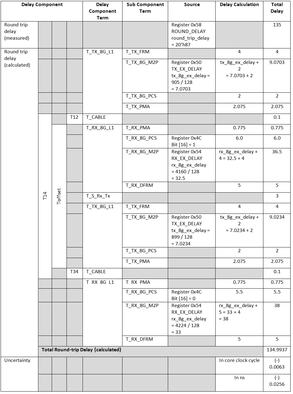
Table 5: Stratix V 9.8304Gbps Total Delay Budget Calculation Example
Table 6: Arria 10 10.1376Gbps Total Delay Budget Calculation Example
Delay calibration
Delay calibration feature is an optional feature for this core, in all of the used cases of this core, they will fulfill the general latency requirement defined by the specification. Should your design latency uncertainty with this IP core does not meet your system latency budget, you could consider the following optional features provided by the core to reduce or eliminate the latency uncertainty. Please note that the quality of the delay calibration is per design case basis.
1)** Round-trip delay (RTD) calibration - An additional soft FIFO is added to the Master Rx side to compensate the changes in round-trip delay, the required user defined round-trip delay can be programmed in register which has a resolution of 1 core clock cycle. Note that during the calibration run phase, this feature will cause the link to go out of Hyperframe synchronization (due to the move of 10ms RFP boundary). For further information on how to use this feature, please refer to the User Guide Chapter 3 Round-Trip Delay Calibration.
2)** Single-trip delay (STD) calibration - Uses an additional PLL to control core clock phase, changes of the core clock phase to the Rx PCS clock will adjust the total variable delay determined by user in register. This feature will not affect the round-trip delay nor the link operation***. However, user should be aware of the UI to step error in measurement that could be introduced when different CPRI rates are used, the resolution of the delay calibration is one-step (1/8 of the VCO period used) of the PLL Dynamic Phase Change feature, see Table 7 below for more information. For information on how-to enable and use this feature, please refer to User Guide Chapter 3 Single-Trip Delay Calibration.
Table 7: Resolution of STD and Calculation of UI to Step Difference
3) Transmitter delay calibration with Tx Bitslip - This feature allows delay changes to the Tx PCS at the resolution of 1UI, if you use this feature the value of the delay (tx_bitslip_in of register XCVR_BITSLIP) added from this feature should be added on top of the T_TX_8G_PCS or T_TX_10G_PCS in Table 2. For more information, please refer to User Guide Chapter 3 Tx Bitslip Delay
Note**: Calibration features 1) and 2) are available from Webcore 16.0 onwards.
Note***: While this feature uses the uplink Tx FIFO to absorb the moving latency, the maximum delay allowed changes should not be more than 12 clock cycles (~70% of Tx FIFO depth). Otherwise, uplink may experience out of Hyperframe synchronization.
Disclaimer
The information provided in this page will only compliant to the latest version of CPRI IP v6 in release page. In addition, these numbers will work in
hardware and there may be discrepancies with simulation model. Should you need further information, please contact engineering.
Community support is provided Monday to Friday. Other contact methods are available here.
Intel does not verify all solutions, including but not limited to any file transfers that may appear in this community. Accordingly, Intel disclaims all express and implied warranties, including without limitation, the implied warranties of merchantability, fitness for a particular purpose, and non-infringement, as well as any warranty arising from course of performance, course of dealing, or usage in trade.
For more complete information about compiler optimizations, see our Optimization Notice.