Constrain SPI Core
Success! Subscription added.
Success! Subscription removed.
Sorry, you must verify to complete this action. Please click the verification link in your email. You may re-send via your profile.
Constrain SPI Core
- Subscribe to RSS Feed
- Mark as New
- Mark as Read
- Bookmark
- Subscribe
- Printer Friendly Page
- Report Inappropriate Content
Constrain SPI Core
This example shows how to constrain a SPI core in a Qsys system.
This example is for the ADIS16209 from Analog Devices: ADIS16209
These are values from the datasheet:
- tDAV = max 100 ns
- tDSU = min 24.4 ns
- tDHD = min 48.8 ns
The SCLK to the ADIS16209 is a generated clock signal, so you need to find out which register generates this clock and then create a generated clock using this register as clock source. You can find the source register for the SCLK signal using the "Report Path..." report command in TimeQuest:
Example for finding source register of generated clock
To get the correct command for the .sdc file use TimeQuest Namefinder: TimeQuest -> View -> Namefinder... and select get_registers under Collection. In this example the Namefinder returned:
[get_registers *qp_sammelplatine:u0\|qp_sammelplatine_peripheral_subsystem:peripheral_subsystem\|qp_sammelplatine_peripheral_subsystem_ADIS16209:adis16209\|SCLK_reg]
In the next step you need to find the source clock which the SPI cores and the clock divider for the SCLK signal. You can find the source clock of the SCLK_reg when you right click on the SCLK_reg signal in the report and select Locate -> Locate in Technology Map Viewer:
Show registers in technology map viewer
and then you can follow the clock signal in the Technology Map Viewer:
Find the clock for a selected register
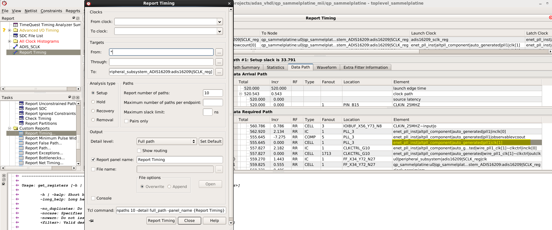
You can also use the Report Timing command from within TimeQuest to find the source clock for the SCLK_reg:
Example for finding the source clock of a register from within TimeQuest
You can determine the clock divider when you divide the source clock rate by the Actual clock rate reported by the SPI properties (double click on the SPI component in Qsys). In this example the clock divider is:
25.000.000 / 961.538 = 26
Now you have everything in place you need to constrain the core:
#**************************************************************
# Constrain ADIS16209
#**************************************************************
# set timing constraints
set Tclk_delay_adis16209_max 1.0
set Tclk_delay_adis16209_min 0.9
set Tsu_adis16209 24.4
set Th_adis16209 48.8
set Tco_adis16209_max 100.0
set Tco_adis16209_min 0.0
# create clocks
set adis16209_clk_divisor 26
create_generated_clock -name adis16209_sclk_reg -source [get_pins {enet_pll_inst|altpll_component|auto_generated|pll1|clk[1]}] -divide_by $adis16209_clk_divisor [get_registers {qp_sammelplatine:u0|*adis16209|SCLK_reg}]
create_generated_clock -name adis16209_sclk_pin -source [get_registers {qp_sammelplatine:u0|*adis16209|SCLK_reg}] [get_ports {ADIS_SCLK}]
# calculate maximum and minimum board delays
set Tclk_delay_adis16209_output_max [expr $Tclk_delay_adis16209_max - $Tclk_delay_fpga_min]
set Tclk_delay_adis16209_output_min [expr $Tclk_delay_adis16209_min - $Tclk_delay_fpga_max]
# apply timing constraints
# data is latched at the rising edge of adis16209_sclk_pin
set_output_delay -add_delay -clock { adis16209_sclk_pin } -max [expr $Tboard_delay_max + $Tsu_adis16209 - $Tclk_delay_adis16209_output_min] [get_ports {ADIS_CS_N ADIS_DIN}]
set_output_delay -add_delay -clock { adis16209_sclk_pin } -min [expr $Tboard_delay_min - $Th_adis16209 - $Tclk_delay_adis16209_output_max] [get_ports {ADIS_CS_N ADIS_DIN}]
# data is launched at the falling edge of adis16209_sclk_pin
set_input_delay -add_delay -clock_fall -clock { adis16209_sclk_pin } -max [expr $Tboard_delay_max + $Tco_adis16209_max - $Tclk_delay_adis16209_output_min] [get_ports {ADIS_DOUT}]
set_input_delay -add_delay -clock_fall -clock { adis16209_sclk_pin } -min [expr $Tboard_delay_min + $Tco_adis16209_min - $Tclk_delay_adis16209_output_max] [get_ports {ADIS_DOUT}]
# set multicycle clock constraints
set_multicycle_path -setup -start -from [get_clocks $enet_clk_25mhz] -to [get_clocks {adis16209_sclk_pin}] [expr $adis16209_clk_divisor/2]
set_multicycle_path -hold -start -from [get_clocks $enet_clk_25mhz] -to [get_clocks {adis16209_sclk_pin}] [expr $adis16209_clk_divisor - 1]
set_multicycle_path -setup -end -from [get_clocks {adis16209_sclk_pin}] -to [get_clocks $enet_clk_25mhz] [expr $adis16209_clk_divisor/2]
set_multicycle_path -hold -end -from [get_clocks {adis16209_sclk_pin}] -to [get_clocks $enet_clk_25mhz] [expr $adis16209_clk_divisor - 1]
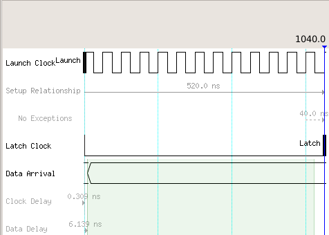
You need the multicycle path constraints because the data register is also clocked by the same clock which clocks the SCLK_reg register. When you look at the timing diagram you can see that the FPGA should launch the data at the falling edge of SCLK and the data is latched at the rising edge of SCLK. Because the FPGA data signal is generated by the same clock which generated the SCLK_reg signal you need to specify a multicycle setup of adis16209_clk_divisor / 2. When you apply the timing constraints the timing looks like this:
Example waveform for constraining a SPI interface (setup)
Example waveform for constraining a SPI interface (hold)
Community support is provided during standard business hours (Monday to Friday 7AM - 5PM PST). Other contact methods are available here.
Intel does not verify all solutions, including but not limited to any file transfers that may appear in this community. Accordingly, Intel disclaims all express and implied warranties, including without limitation, the implied warranties of merchantability, fitness for a particular purpose, and non-infringement, as well as any warranty arising from course of performance, course of dealing, or usage in trade.
For more complete information about compiler optimizations, see our Optimization Notice.