Generating and Modifying IBIS files for Arria 10 EMIF
Änderungen angenommen. Das Abonnement wurde hinzugefügt.
Erfolgreiche Durchführung! Abonnement entfernt.
Sie müssen sich verifizieren, um diese Aktion abzuschließen. Klicken Sie auf den Verifizierungslink in Ihrer E-Mail. Erneut senden über Ihr Profil.
- Intel Community
- Intel Community Wissensdatenbank
- Product Support Forums Wissensdatenbank
- FPGA Wissensdatenbank
- FPGA Wiki
- Generating and Modifying IBIS files for Arria 10 EMIF
Generating and Modifying IBIS files for Arria 10 EMIF
- RSS-Feed abonnieren
- Als neu kennzeichnen
- Als gelesen kennzeichnen
- Lesezeichen
- Abonnieren
- Drucker-Anzeigeseite
- Anstößigen Inhalt melden
Generating and Modifying IBIS files for Arria 10 EMIF
Generating IBIS files using Quartus
- Create an external memory interface project in Quartus.
- Open the project in Quartus v14.0 or above.
- Select Assignments > Settings.
- On the left panel under Category, select EDA Tool Settings > Board-Level.
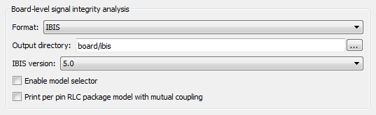
- Under Board-level signal integrity analysis, select the following:

3/3b/Board-level_signal_integrity_analysis_setup .png ( Board-level signal integrity analysis setup.png - click here to view the image )
Board-level signal-integrity analysis setup for IBIS file generation.
After compilation, navigate to the directory where the project is located and open the folder named board. Inside will be another folder labeled ibis, which will contain the generated IBIS file.
Modifying IBIS files for External Memory Interface Simulation
Open your FPGA IBIS model in your favorite text editor.
To change the measurement location from the Pin to the Die
Add the following lines under [Component]:
Si_location Die
Timing_location Die
To change the Voltage Thresholds
This is NOT applicable for DDR4
Find the I/O standard name associated with the DQ net group. For example, for a DDR3 DQ pin with the SSTL 15 I/O standard, you might see something like sstl15_rtnio_g120c_r34c. Find the area where the I/O standard model description is located. Change the Vinl and Vinh values to +/- 70mV of Vref under the Enable Active-Low and [Model Spec] lines.
If Vref = 0.75V, then change the Vinl and Vinh values under the Enable Active-Low line to the following values:
| Vinl | = 0.680 | |
| Vinh | = 0.820 |
And change the Vinh and Vinl values under the [Model Spec] line to the following values:
| Vinh | 0.820 | 0.820 | 0.820 | ||||
| Vinl | 0.680 | 0.680 | 0.680 |
For DDRx Batch Wizard Only
When using the DDRx Batch Simulation Wizard, some warnings may be encountered if the I/O standard name of a given net group (DQ, DQS, or Address/Command/Control) does not match. To address these warnings all the DQ, DM, and Address/Command/Control pins need to have the same model name.
To ensure each net group contains matching model names, make the following changes:
1. Change the model_name for all the DQ, DM, and Address/Command/Control signals from <Interface Standard>_rtnio_<OCT>_<Driver> to
<Interface Standard>_rtpio_<OCT>_<Driver>.
2. Change the model_name for the reset_n signal to match that of the DQ, DM, and Address/Command/Control signals (change the Interface Standard and Differential).
3. Applicable only if you have enabled model selector. The suffixes for every given net group (DQ, DQS, and Address/Command/Control) must be the same. For example, if your DQ0 signal is named pod12_rtpio_g40c_r34cp1_lv_ms8 and DQ1 is named pod12_rtnio_g40c_r34cp1_lv_ms9, make sure that all the DQ pins are named pod12_rtpio_g40c_r34cp1_lv_ms8.
Community-Support wird während der normalen Geschäftszeiten (Montag bis Freitag, 7.00 bis 17.00 Uhr PST) angeboten. Andere Kontaktmethoden finden Sie hier.
Intel überprüft nicht alle Lösungen, darunter auch nicht alle Dateiübertragungen, die ggf. in der Community stattfinden. Dementsprechend lehnt Intel alle ausdrücklichen und stillschweigenden Garantien ab, einschließlich und ohne Einschränkung stillschweigender Garantien der Marktgängigkeit, der Eignung für einen bestimmten Zweck und der Nichtverletzung von Rechten sowie jeglicher Garantien, die sich aus der Ausführung, Bearbeitung oder handelsmäßigen Verwendung ergeben.
Vollständige Angaben zu Compiler-Optimierungen finden Sie in unseren Optimierungshinweis.