How to use Onchip debug tool kit in External Memory Interface Designs
Success! Subscription added.
Success! Subscription removed.
Sorry, you must verify to complete this action. Please click the verification link in your email. You may re-send via your profile.
- Intel Community
- Intel Community Knowledge Base
- Product Support Forums Knowledge Base
- FPGA Knowledge Base
- FPGA Wiki
- How to use Onchip debug tool kit in External Memory Interface Designs
How to use Onchip debug tool kit in External Memory Interface Designs
- Subscribe to RSS Feed
- Mark as New
- Mark as Read
- Bookmark
- Subscribe
- Printer Friendly Page
- Report Inappropriate Content
How to use Onchip debug tool kit in External Memory Interface Designs
Introduction
On Chip Debug Toolkit is simply an Avalon port into the sequencer memory to debug your external memory design. It allows user logic to access the sequencer to retrieve calibration information and run commands. On chip debug toolkit can be used for live in-system monitoring of calibration data.
When to use Onchip Tool kit vs EMIF Debug toolkit
EMIF debug toolkit also provides calibration data. However, it may be difficult to use during volume/production testing. On chip toolkit is extremely useful during volume testing, when multiple boards are connected to multiple PCs to raise a flag when the calibration margins are not matching expected results. State machine can be used in the FPGA itself to raise a flag.
For more information about On Chip toolkit refer to Handbook link below (Chapter 13-8)
http://www.altera.com/literature/hb/external-memory/emi_uniphy_ref_EMIF_toolkit.pdf
The wiki page describes the steps to create a DDR3 design that uses On chip debug tool kit.
System Features
Quartus II software version 13.0.
Stratix V FPGA Development kit with a JTAG connected to the PC.
System Block diagram for Onchip debug Tool kit
0/04/Toolkit_snapshot1.JPG ( Toolkit snapshot1.JPG - click here to view image )
Step by Step Instruction on how to add On Chip Debug Toolkit and use it for Memory Interface Debug
1. Launch QSYS from Quartus. (Tools → QSYS)
2. Add the following components from the Component Library.
a. On-Chip Memory, this component is to be used as instruction memory.
i. Select 32-bit width, 131072 bytes.
b. On-Chip Memory, this component to be used as data memory.
i. Select 32-bit width, 131072 bytes.
c. Nios II/f processor.
i. Set Reset vector memory to the instruction memory instance.
ii. Set Exception vector memory to the instruction memory instance.
iii. In JTAG Debug module Debug tab set level 4 (required for software debug).
d. JTAG UART, this component is for stdout/stdin/stderr functionality.
i. Ensure that Buffer Depth for Read and Write FIFO is 64 bytes.
e. DDR3 SDRAM Controller with UniPHY.
i. Ensure that IP settings are set correctly as per design intention.
ii. In Diagnostics tab, select Debug option1 and Enable EMIF On-chip Debug toolkit.
Selecting these options ensures that core_debug.h and core_debug_defines.h are generated in <design_name>/<design_name>_s0_software folder during UniPHY IP generation. "core_debug_defines.h" is header file that defines directives for UniPHY IP settings. "core_debug.h" is header file that defines commands and data structures for retrieving debug information.
f. Avalon-MM Traffic generator.
i. Modify Traffic generation and pattern settings as required.
3. The complete system should be connected as the diagram below illustrates.
Note that if base addresses are overlapping, you need to re-assign them. (System→Assign Base addresses)
8/8b/Qsys_onchip_design_1.JPG ( Qsys onchip design 1.JPG - click here to view image )
4. Select the correct device and family under the “Project Settings” tab.
5. Name and save your QSYS system. E.g. “DDR3_onchip”.
6. From Generation tab, select Generate to create the QSYS system. (Generation tab→Generate)
7. Create a Quartus II project; note that you should use the same device as in your Qsys system.
8. Add the QIP file generated by QSYS to your Quartus II project.
9. Open a new verilog file and instantiate the DDR3 interface, the Nios system, and connect the ports as it is shown below.
Add this Verilog file in the Project and set this file as Top-Level entity. (Project tab → Add/Remove files in Project . Right click the file to set as Top- Level entity).
[[1] ]
Note that DDR3_onchip_top.v is an top level entity example for DDR3 800MHz x72 design.
10. Open a new SDC file, define your clock as it is shown below, and save and name it in your Quartus II project. E.g. “DDR3_onchip_nios.sdc”
In this design, the input clock is at 100MHz.
create_clock -period 10 -waveform [ list 0 5 ] "clk"
11. Add pin location and I/O standard assignment for the top-level design.
12. Compile project to generate SOF and make sure timing is closed.
13. Program the FPGA.
14. From Quartus, select Tools → Nios II Software Build Tools for Eclipse.
15. Create a new workspace if prompted. Note that selecting default workspace may lead to using incorrect workspace.
16. From Nios II Eclipse window, select tab File → New → Nios II Application and BSP from Template.
17. QSYS should have created a .sopcinfo file during generation. Select the file for the “SOPC Information File name” field. Once selected Eclipse will try to automatically load all the CPU settings. Note that It is important to select the correct .sopcinfo file.
18. Specify desired project name. E.g. “nios2_sequencer_example”.
19. Specify “Blank Project” as the “Project Template” and Click “Finish” to generate project.
20. From Nios II Eclipse Project explorer, right click the project folder and select new file and Enter the file name “Onchip_Toolkit_debug.c” .
21. Copy the C code from Onchip_Toolkit_debug.c in the link below.
[[2] ]
22. From Windows explorer, find the core_debug.h and core_debug_defines.h header files in
<design_name>/<design_name>_s0_software/sequencer and include these files in your debug component code.
23. Copy files sequencer.h, sequencer_defines.h , core_debug.h, core_debug_defines.h in the same folder where the debug C code file resides.
24. From Quartus II project window select Project → Build All, make sure there is no error. At this point you should have a .elf file generated under your software directory. This is the build result. Note that there will be errors, if the header files are not copied as described above.
25. From Nios II Eclipse window, Select Run → Debug Configurations.
26. Select “Nios II Hardware → New Configurations.
27. Select “Project name” and ELF file name. You may need to select “Enable browse for file system ELF file” and select the file explicitly.
(The .elf file (which is located inside “Application” Project Folder) contains all the compiled output codes (in “executable, linkable format”). This is what gets downloaded to the board. The system.h file (which is located inside the “BSP” Project Folder, is the System description header file. It contains the memory map of all the peripherals in the system and their symbolic names. )
28. Go to “Target Connection” and make sure exactly one processor is listed under the Processors list and one JTAG UART is listed under the Byte Stream Devices. If this isn’t true, make sure the board is connected properly to the PC and make sure you’ve programmed the SOF to the FPGA.
29. You may need to select “Ignore mismatched system ID” and “Ignore mismatched system timestamp” if the “Debug” button is disabled.
30. Click Apply, then Debug.
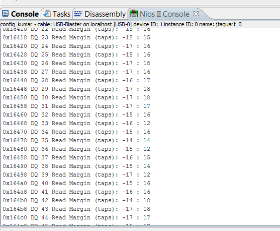
31. You should now be able to see the custom calibration reports in the “Nios II Console” window.
0/06/NiosII_console.png ( NiosII console.png - click here to view image )
32. Remember that anytime you go back to change the QSYS system, you need to re-generate it, recompile the QII project, reprogram the SOF, and re-create the software project (since you likely have modified the address spaces).
Information on the files used in Onchip toolkit design
| Files | Description | Location |
|---|---|---|
| Sequencer.h | is header file that defines calibration stages/ sub stages and bases addresses for different managers (PHY, Data, Scan chain) within the UniPHY | <design_name>/<design_name>_s0_software |
| Sequencer_defines.h | is header file that defines UniPHY IP settings | <design_name>/<design_name>_s0_software |
| core_debug.h | is header file that defines commands and data structures for retrieving debug information. | <design_name>/<design_name>_s0_software |
| core_debug_defines.h | is header file that defines UniPHY IP settings | <design_name>/<design_name>_s0_software |
| system.h | is the System description header file. It contains the memory map of all the peripherals in the system and their symbolic names | inside the “BSP” Project Folder |
| .elf | contains all the compiled output codes in “executable, linkable format" | inside “Application” Project Folder |
Community support is provided during standard business hours (Monday to Friday 7AM - 5PM PST). Other contact methods are available here.
Intel does not verify all solutions, including but not limited to any file transfers that may appear in this community. Accordingly, Intel disclaims all express and implied warranties, including without limitation, the implied warranties of merchantability, fitness for a particular purpose, and non-infringement, as well as any warranty arising from course of performance, course of dealing, or usage in trade.
For more complete information about compiler optimizations, see our Optimization Notice.