Intro to Altera SoC Devices for HW Developers Workshop - Add FPGA Peripherals
Success! Subscription added.
Success! Subscription removed.
Sorry, you must verify to complete this action. Please click the verification link in your email. You may re-send via your profile.
- Intel Community
- Intel Community Knowledge Base
- Product Support Forums Knowledge Base
- FPGA Knowledge Base
- FPGA Wiki
- Intro to Altera SoC Devices for HW Developers Workshop - Add FPGA Peripherals
Intro to Altera SoC Devices for HW Developers Workshop - Add FPGA Peripherals
- Subscribe to RSS Feed
- Mark as New
- Mark as Read
- Bookmark
- Subscribe
- Printer Friendly Page
- Report Inappropriate Content
Intro to Altera SoC Devices for HW Developers Workshop - Add FPGA Peripherals
In this section you will use QSys to add and configure FPGA pre-existing peripherals to your SoC system, create and add a custom peripheral to your system, assign addresses for these peripherals, connect the clocks and resets, and generate the RTL for the system.Overview
<<<<Click here to return to the previous section
Adding Pre-built FPGA Peripherals
In this lab, all FPGA clocks and resets will be sourced from the HPS. Therefore, you don't need a clock source function in the QSys system.
1. In the QSYs GUI, select the "clk_0" Clock Source, right click, and select "Remove" to delete this function.
Soc_hw_ws_files9.jpg (Click here for image)
2. Now you will add an on-chip RAM to your system and connect it to the high-performance HPS to FPGA bridge AXI interface.
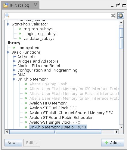
- In the "IP Catalog" in the upper left-hand corner of QSys, go under "Library", expand "Basic Functions", under that expand "On Chip Memory", select "On-Chip Memory (RAM or ROM), and click the "Add..." button.
Soc_hw_ws_files10.jpg (Click here for image)
3. In the window which pops up:
- Change "Data width:" to 64 to match the width you configured in the HPS GUI
- Change the "Total memory size:" to 2048 bytes.
- Uncheck the "Initialize memory content" checkbox
- Keep all the other defaults, then click "Finish" to complete adding this component to your system.
Soc_hw_ws_files11.jpg (Click here for image)
4. Now you will add a System ID Peripheral. The System ID Peripheral provides a unique identification number and time stamp to allow SW to verify the version of FPGA hardware being use.
- In the "IP Catalog" search field, type "System ID Peripheral"
- Select the "System ID Peripheral" and click the "Add..." button.
- Leave the default settings and click "Finish" in the System ID Peripheral component window.
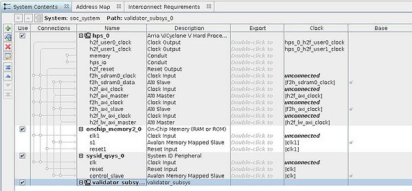
5. The last pre-build peripheral you will add is the workshop validator system. This is the peripheral used by the verification utility to sign the files which verify you've fully completed the workshop.
- Under the "Project section of the "IP Catalog", expand "Workshop Validator", select "validator_subsys", click the "Add..." button, then click "Finish" in the validator_subsys component window.
Soc_hw_ws_files12.jpg (Click here for image)
Creating and Adding custom FPGA Peripheral
Now you will create a QSys component based on RTL source code and add that component into your QSys system. The pre-written module provided for the lab uses an Altera Avalon bus interface. When the signals names of a supported bus interface are properly
1. At the bottom left corner of the QSys IP Catalog window, click the "New..." button. This will bring up the QSys "Component Editor" window.
2. In the "Component Type" tab of the "Component Editor" window, make the following changes:
- Enter "lab_module" in the "Name:" field.
- Enter "Lab Module" in the "Display Name:" field.
- Enter "Lab Components" in the "Group:" field.
3. In the Component Editor window, click the "Files" tab. In this tab, do the following:
- Under "Synthesis Files", click the "Add File..." button.
- In the Add File window, select the file "lab_module.sv" from the project directory, then click "Open". The file "lab_module.sv" should now appear in the "Synthesis Files" table.
- Click the "Analyze Synthesis Files" button and wait for the analysis to complete.
Soc_hw_ws_files13.jpg (Click here for image)
4. Click the "Parameters" tab in the "Component Editor" window. You will see that two parameters "ADDW" and "DATW" have been populated from parameters specified in the file "lab_module.sv".
5. Click the "Signals & Interfaces" tab in the Component Editor window. You will see that the clock, reset, and Avalon Memory Mapped Slave interface have all been populated by analyzing the IO in the source file. However, the Component Editor has not associated the AV-MM Slave with the reset input.
- Change the "Associated Reset:" drop-down field to "reset".
- All of the other defaults are acceptible, so click the "Finish..." button in the component Editor
- Click "Yes, Save" to save your new component.
You have now built a custom QSys component which can be instantiated in your system.
Soc_hw_ws_files14.jpg (Click here for image)
6. Finally, you will instantiate your new component. In the IP Catalog window, under "Project", expand "Lab Components", select "Lab Module", click the "Add..." button, then clock "Finish" in the Lab Module component window. You system should now look like this.
Soc_hw_ws_files15.jpg (Click here for image)
Connecting the Clocks and Resets
Next you will connect the clocks and resets for your QSys system. In this lab, we will connect all interfaces to the 50MHz h2f_user1_clock. In areas of a system where performance is important, you would likely run the high performance HPS to FPGA, FPGA to FPGA, and FPGA to SDRAM bridges at a higher clock frequency and run only the lightweight HPS to FPGA bridge at slower clock rate. However, for the purposes of this lab, 50MHz for the system will suffice.
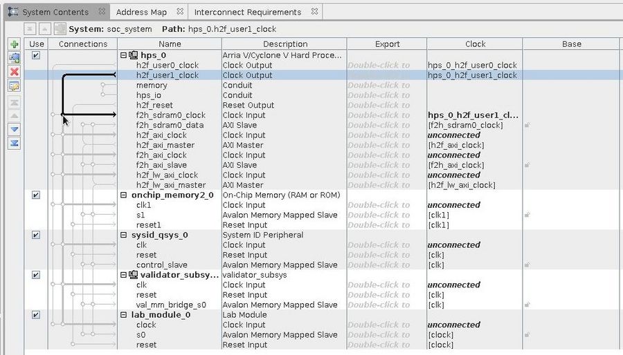
1. In the QSys "System Contents" tab, under the "hps_0" component, select the "h2f_user1_clock" signal. This will highlight it's connection to the rest of the system.
2. For all of the "Clock Input" signals on all of the components, including "hps_0", use the pointer to enable the connection by clicking the empty circle where the h2f_user1_clock" signal intersects each "Clock Input" signal, as show below.
Note: there will be delay between when you click and when the connection appears.
Soc_hw_ws_files16.jpg (Click here for image)
- Be certain to complete the clock connections for all component clock inputs.
3. Under the "hps_0" component, select the "h2f_reset" Reset Output signal, then connect this signal to the "Reset Input" signals of the four slave components.
Soc_hw_ws_files17.jpg (Click here for image)
Connecting the HPS to the FPGA Peripherals and Assigning Addresses
You will connect the HPS AXI bridge masters to the Avalon-MM ports of the FPGA slaves. As the QSys fabric will automatically translate between supported memory mapped bus standards, no AXI to Avalon bridges are required.
1. Connect the On-Chip RAM to the HPS-to-FPGA high performance bridge.
- On the "hps_0" component, select the "h2f_axi_master" output.
- Enable the connection from the "h2f_axi_master" to the "s1" port of the "onchip_memory2_0" component.
2. Connect the HPS to FPGA Lightweight bridge to the other three components in the system.
- On the "hps_0" component, select the "h2f_lw_axi_master" output.
- Enable the connection from the "h2f_lw_axi_master" to the Avalon Memory Mapped Slave ports of the three remaining peripherals.
- Your system should now look like this:
Soc_hw_ws_files18.jpg (Click here for image)
3. Now you will set the base addresses for the FPGA peripherals. These base addresses are the offsets from the address of the HPS/FPGA bridge to which the peripherals are attached. Set the following addresses by double clicking on the address in the "Base" column next to each perpheral in the "System Contents" window.
- Set the base address of "onchip_memory2_0" to 0x0000_0000
- Set the base address of "sysid_qsys_0" to 0x0000_1000
- Set the base address of "validator_subsys_0" to 0x0001_0000
- Set the base address of "lab_module_0" to 0x0004_0000
Be certain that these addresses are correct. If they are not, the pre-compiled validator component won't function properly.
Soc_hw_ws_files19.jpg (Click here for image)
Export HPS Peripheral IO
Finally, you wil export the HPS peripheral IO from the QSys system.
1. In the QSys "System Contents" window, under "hps_0", find the "memory" conduit. In the "Export" column, double click on "Double-click to export" in the "memory" conduit row. The exported interface name should show up as "memory".
2. In the QSys "System Contents" window, under "hps_0", find the "hps_io" conduit. In the "Export" column, double click on "Double-click to export" in the "memory" conduit row. Change the name of the exported interface to "hps_0_hps_io".
It is important that these names are correct as these names are used in the top-level module for the project.
Your final QSys system should look like this:
Soc_hw_ws_files20.jpg (Click here for image)
Save and Generate your QSys System
1. From the QSys "Generate" menu, select "Generate HDL..."
2. In the "Generation" dialog box, keep the default. The project as implemented uses Verilog. For your own custom designs, you can select either Verilog or VHDL.
3. Click the "Generate" button.
4. When generation is complete, click the "Close" button and continue with the next section of the lab.
Community support is provided during standard business hours (Monday to Friday 7AM - 5PM PST). Other contact methods are available here.
Intel does not verify all solutions, including but not limited to any file transfers that may appear in this community. Accordingly, Intel disclaims all express and implied warranties, including without limitation, the implied warranties of merchantability, fitness for a particular purpose, and non-infringement, as well as any warranty arising from course of performance, course of dealing, or usage in trade.
For more complete information about compiler optimizations, see our Optimization Notice.