Low Latency Ethernet 10G MAC using Arria 10 PHY 10GBASE-R Register Mode
Success! Subscription added.
Success! Subscription removed.
Sorry, you must verify to complete this action. Please click the verification link in your email. You may re-send via your profile.
- Intel Community
- Intel Community Knowledge Base
- Product Support Forums Knowledge Base
- FPGA Knowledge Base
- FPGA Wiki
- Low Latency Ethernet 10G MAC using Arria 10 PHY 10GBASE-R Register Mode
Low Latency Ethernet 10G MAC using Arria 10 PHY 10GBASE-R Register Mode
- Subscribe to RSS Feed
- Mark as New
- Mark as Read
- Bookmark
- Subscribe
- Printer Friendly Page
- Report Inappropriate Content
Low Latency Ethernet 10G MAC using Arria 10 PHY 10GBASE-R Register Mode
February 6, 2015
Last Major Update
Introduction
This design example demonstrates Low Latency 10G Ethernet IP solution for Arria 10® using Altera® Low Latency 10-Gbps Ethernet (10GbE) Media Access Controller (MAC) and Native PHY IP cores with small form factor pluggable plus (SFP+). It is capable to achieve low roundtrip latency, 136.677ns (time taken to transmit the first data from Avalon-ST TX interface to be available at Avalon-ST RX interface) in the simulation. Besides,it supports packet monitoring system on transmit and receive paths and report Ethernet MAC statistics counter for transmit and receive data paths.
Other Low Latency Ethernet 10G MAC reference designs:
1. AN701:Scalable Low Latency Ethernet 10G MAC using Arria 10 1G/10G PHY
2. Single Port LL Ethernet 10G MAC with 1588 using Native PHY Design Example
3. Scalable LL Ethernet 10G MAC with 10G BaseR PHY Design Example
Note: This design example can be generated from the Low Latency Ethernet 10G MAC IP Parameter Editor of which can be invoked from IP Catalog beginning with Quartus Prime v15.1. User can apply the "10GBase-R Register Mode Example Design" preset at the right bottom corner of Low Latency Ethernet 10G MAC IP Parameter Editor to generate this design example. Refer to Design Examples for Low Latency 10G Ethernet MAC User Guide for more information.
Design Examples components
Table 1: Table1.png (Click here for image)
Clocking and reset scheme
The following diagram shows the clocking and reset scheme for the design example. At the top-level of the design, there are two external clock sources, ref_clk_clk (322.265625MHz) and csr_clk (100MHz)and one master reset, master_reset_n. The master reset is asynchronous and active low reset signal. This reset signal is then synced to different clock domain internally. When the master_reset_n is asserted, it brings down all modules in the design example.
Figure 1: Clock%26reset_scheme.png (Click here for image)
Interface signals
Table 2: Interfacesignals.png (Click here for image)
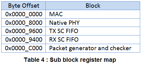
Register Map
All register space for this example design is 32 bit. The following tables show the address offset for the design example and client logic at the top-level of the design.
Table 3: Designblockregmap.png (Click here for image)
Table 4: Subblockregmap.png (Click here for image)
Testbench Files
Table 5: Testbenchfiles.png (Click here for image)
Software and Hardware Requirements
Altera uses the following software and hardware to test the design examples:
■ Altera Complete Design Suite(ACDS) version 14.1A10S
■ ModelSim-SE 10.3c
■ Altera Arria 10 GX SI Development Board (10AX115S4F45I3SGE2)
■ Clock Control ( The Clock Control tool is shipped with the “Installation Kit” for Arria 10 GX SI Development Board )
Procedures to simulate the design with ModelSim-SE software
Testbench_setup.png (Click here for image)
Testbench is included in the design example package for simulation verification. Below are the steps to run the simulation:
1. Download and restore the design example: LL-Ethernet-10G-A10-phy-10GBaser-Register-mode.
2. Launch Modelsim-SE 10.3c and change the directory to LL_Ethernet_10G_A10_phy_10GBaser_Register_mode\testbench.
3. In the TCL console window, type the below command:
tb_run.tcl
4. At the end of the simulation, Modelsim simulator will generate statistics of transmitted packets and received packets in the Transcript window. While in the Wave window, the roundtrip latency for serial loopback is indicated by the measurement cursors that show the time taken to transmit the first data from Avalon-ST TX interface to be available at Avalon-ST RX interface.
Figure 2: Txstatistics.png (Click here for image)
Figure 3: Rxstatistics.png (Click here for image)
Figure 4: VLL_simulation.png (Click here for image)
Procedures to run the hardware design
The design example package comes with pre-generated RTL files that implement a single Ethernet channel uses the on-board small form factor pluggable plus (SFP+). Below are the steps to perform hardware test:
1. Download and restore the design example: (refer to the project link above).
2. Launch the Quartus II 14.1A10S software and then open the project file, “altera_eth_top.qpf”.
3. Run full compilation for the design example. A “.sof” file will be generated once the compilation is complete.
4. Configure the FPGA on Arria 10 GX SI Development Board using the generated, “altera_eth_top.sof” file.
5. After configuration is done, open the Clock Control tool, “ClockControl.exe”. The Clock Control tool is shipped with the “Installation Kit” for Arria 10 GX SI Development Board.
6. Set the new frequency for Y5 and Y6 as shown below:
Y5.png (Click here for image)
Y6.png (Click here for image)
7. Press User Push Button S1 to reset the system.
Note: System must be hard reset after configuration done.
8. On Quartus II Tools menu, click on System Debugging Tools and then launch System Console.
9. In the System Console command shell, change the directory to “LL_Ethernet_10G_A10_phy_10GBaser_Register_mode/script”.
10. Perform the following test by running the command in the System Console command shell:
a. SFP+ loopback
Command:
i. source gen_conf.tcl (Generate and send 0xffff2000 packets)
ii. source monitor_conf.tcl (To check the number of good and bad packets received)
iii. source show_stats.tcl (To show the statistics counter values)
b. Avalon-ST loopback
Command: source loopback_conf.tcl (enable Avalon-ST loopback)
Disclaimer
© [2013] Altera Corporation. The material in this wiki page or document is provided AS-IS and is not supported by Altera Corporation. Use the material in this document at your own risk; it might be, for example, objectionable, misleading or inaccurate.
Community support is provided during standard business hours (Monday to Friday 7AM - 5PM PST). Other contact methods are available here.
Intel does not verify all solutions, including but not limited to any file transfers that may appear in this community. Accordingly, Intel disclaims all express and implied warranties, including without limitation, the implied warranties of merchantability, fitness for a particular purpose, and non-infringement, as well as any warranty arising from course of performance, course of dealing, or usage in trade.
For more complete information about compiler optimizations, see our Optimization Notice.