Lowering Cyclone V power using different I/O standard for LPDDR2
Success! Subscription added.
Success! Subscription removed.
Sorry, you must verify to complete this action. Please click the verification link in your email. You may re-send via your profile.
- Intel Community
- Intel Community Knowledge Base
- Product Support Forums Knowledge Base
- FPGA Knowledge Base
- FPGA Wiki
- Lowering Cyclone V power using different I/O standard for LPDDR2
Lowering Cyclone V power using different I/O standard for LPDDR2
- Subscribe to RSS Feed
- Mark as New
- Mark as Read
- Bookmark
- Subscribe
- Printer Friendly Page
- Report Inappropriate Content
Lowering Cyclone V power using different I/O standard for LPDDR2
This wiki page has been created to show users an additional way to reduce power on designs that use LPDDR2 external memory with Cyclone V. The method applies to both Cyclone V hard memory controller (HMC) and soft memory controller (SMC).
Creating an LPDDR2 external memory controller using the Megawizard or Qsys flow in Cyclone V defaults to using 1.2V HSUL I/O standards. Using the Cyclone V E development kit and two example designs, this article will detail how to reduce power on the bidirectional 1.2V HSUL standard used to interface the data input and output to and from the LPDDR2 memory.
First, start with the zipped design below that uses HSUL 1.2V for the LPDDR2 DQ pins. The design was created by using the Megawizard to generate an LPDDR2 SMC at 300Mhz with example project. The example project qsf file was then adjusted to match the pinout locations on the Cyclone V E devkit. A compile was performed, than the tcl file was run to do pin assignments. Finally, the loop variable in the *_do.v file was changed to allow the test pattern generator and checker to run infinitely rather than stop after a finite amount of time specified by loop > 0.
13.0 Design using 1.2V HSUL for LPDDR2 DQ pins
File:Lpddr2x16 smc loop0 13.0.zip
The loop variable change can be seen in the following line with the comment suffix below (file: ./submodules/<project_name>_d0.v)
driver_avl_use_be_avl_use_burstbegin #(
  .DEVICE_FAMILY ("Cyclone V"),
  .TG_AVL_DATA_WIDTH (64),
  .TG_AVL_ADDR_WIDTH (27),
  .TG_AVL_WORD_ADDR_WIDTH (24),
  .TG_AVL_SIZE_WIDTH (3),
  .TG_AVL_BE_WIDTH (8),
  .DRIVER_SIGNATURE (1431634050),
  .TG_GEN_BYTE_ADDR (1),
  .TG_NUM_DRIVER_LOOP (0), // Change from 1 to 0 for infinite traffic generation and checking
  .TG_ENABLE_UNIX_ID (0),
  .TG_USE_UNIX_ID (0),
  .TG_RANDOM_BYTE_ENABLE (1),
  .TG_ENABLE_READ_COMPARE (1),
  .TG_POWER_OF_TWO_BURSTS_ONLY (0),
  .TG_BURST_ON_BURST_BOUNDARY (0),
  .TG_DO_NOT_CROSS_4KB_BOUNDARY (0),
  .TG_TIMEOUT_COUNTER_WIDTH (32),
  .TG_MAX_READ_LATENCY (20),
  .TG_SINGLE_RW_SEQ_ADDR_COUNT (32),
  .TG_SINGLE_RW_RAND_ADDR_COUNT (32),
  .TG_SINGLE_RW_RAND_SEQ_ADDR_COUNT (32),
  .TG_BLOCK_RW_SEQ_ADDR_COUNT (8),
  .TG_BLOCK_RW_RAND_ADDR_COUNT (8),
  .TG_BLOCK_RW_RAND_SEQ_ADDR_COUNT (8),
  .TG_BLOCK_RW_BLOCK_SIZE (8),
  .TG_TEMPLATE_STAGE_COUNT (4),
  .TG_SEQ_ADDR_GEN_MIN_BURSTCOUNT (1),
  .TG_SEQ_ADDR_GEN_MAX_BURSTCOUNT (4),
  .TG_RAND_ADDR_GEN_MIN_BURSTCOUNT (1),
  .TG_RAND_ADDR_GEN_MAX_BURSTCOUNT (4),
  .TG_RAND_SEQ_ADDR_GEN_MIN_BURSTCOUNT (1),
  .TG_RAND_SEQ_ADDR_GEN_MAX_BURSTCOUNT (4),
  .TG_RAND_SEQ_ADDR_GEN_RAND_ADDR_PERCENT (50)
) traffic_generator_0 (
  .pass (pass), // status.pass
  .fail (fail), // .fail
  .test_complete (test_complete), // .test_complete
  .clk (clk), // avl_clock.clk
  .reset_n (reset_n), // avl_reset.reset_n
  .avl_ready (avl_ready), // avl.waitrequest_n
  .avl_addr (avl_addr), // .address
  .avl_size (avl_size), // .burstcount
  .avl_wdata (avl_wdata), // .writedata
  .avl_rdata (avl_rdata), // .readdata
  .avl_write_req (avl_write_req), // .write
  .avl_read_req (avl_read_req), // .read
  .avl_rdata_valid (avl_rdata_valid), // .readdatavalid
  .avl_be (avl_be), // .byteenable
  .avl_burstbegin (avl_burstbegin), // .beginbursttransfer
  .pnf_per_bit (), // (terminated)
  .pnf_per_bit_persist (), // (terminated)
  .csr_address (13'b0000000000000), // (terminated)
  .csr_write (1'b0), // (terminated)
  .csr_writedata (32'b00000000000000000000000000000000), // (terminated)
  .csr_read (1'b0), // (terminated)
  .csr_readdata (), // (terminated)
  .csr_waitrequest (), // (terminated)
  .csr_be (4'b0000) // (terminated)
);
It was changed from 1 to 0 to allow infinite testing. Keep in mind that drv_status_test_complete and drv_status_pass will not transition high. Instead, the test should run without ever seeing test fail. drv_status_fail, drv_status_pass, and drv_status_test_complete are status signals from the traffic generator and checker.
Below is a snapshot of relevant signals in SignalTap to make sure the controller is running error free. The pnf (pass not fail) bits should stay all Fs. If any of the bits transitions low on the persistent bits, an error has been detected.

LPDDR2 example design traffic checker status and Avalon signals
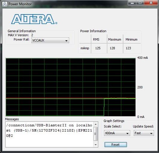
After verifying via SignalTap that the design is running and passing traffic via Autorun analysis, stop Autorun. The PowerMonitor.exe board test system executable was then run to measure power on all voltage rails.
Here is a snapshot of the PowerMonitor GUI

PowerMonitor GUI
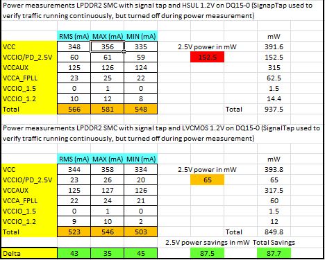
Below are the results for the baseline design using HSUL 1.2V for the LPDDR2 DQ pins.

HSUL 1.2V for the LPDDR2 DQ pins.
The project above was then copied. The directory was renamed to lpddr2x16_smc_LVCMOS_dq_loop0. To convert the DQ I/O from HSUL to LVCMOS, two file changes are required.
13.0 Design using 1.2V LVCMOS for LPDDR2 DQ pins
File:Lpddr2x16 smc LVCMOS dq loop0 13.0.zip
The first file that needs to be changed is the project qsf file. All mem_dq pins were changed from "DIFFERENTIAL 1.2-V HSUL" to "1.2 V" for 1.2V LVCMOS.
i.e.
From:
set_instance_assignment -name IO_STANDARD "1.2-V HSUL" -to mem_dq[0]
to:
set_instance_assignment -name IO_STANDARD "1.2 V" -to mem_dq[0]
Then, all associated output termination was removed from the dq pins.
i.e. Remove all lines associated with mem_dq[*]
set_instance_assignment -name OUTPUT_TERMINATION "SERIES 34 OHM WITH CALIBRATION" -to mem_dq[0]
A user can diff the two qsf project files in this wiki page to understand the changes made.
The second file that needs to be changed is called ./submodules/altdq_dqs_acv_cyclonev_lpddr2.sv. One line of code should be removed to not allow series termination control on the bidirectional I/O associated with the LPDDR2 memory controller I/O.
  else if (PIN_TYPE == "bidir")
    begin
      cyclonev_io_obuf
      #(
        .sim_dynamic_termination_control_is_connected("false")
      ) data_out (
        .oe (~delayed_oe),
        .i (delayed_data_out),
        .o (read_write_data_io [pin_num]),
        // .seriesterminationcontrol (seriesterminationcontrol_in),
        .obar(),
        .devoe()
      );
Once the above changes have been made, re-compile the design.
Download the sof file and bring up SignalTap again to verify that the memory has calibrated and is running error free. The following spreadsheet shows the difference in power consumption using 1.2V LVCMOS vs. 1.2V HSUL. Savings is almost 90mW! Other examples have seen in upwards of 100mW savings for LPDDR2 interfaces that are 16 bits wide. Savings will be higher for wider LPDDR2 memories.

LVCOMS 1.2V for the LPDDR2 DQ pins.
Power savings is seen in the 2.5V VCCPD power supply since bidirectional HSUL, SSTL, and SSTLII use the pre-driver supply while LVCMOS does not.
Special thanks go out o Andy O'Reilly for proposing this great idea and getting characterization data from the folks in Altera Engineering (SR#10894759).
Community support is provided during standard business hours (Monday to Friday 7AM - 5PM PST). Other contact methods are available here.
Intel does not verify all solutions, including but not limited to any file transfers that may appear in this community. Accordingly, Intel disclaims all express and implied warranties, including without limitation, the implied warranties of merchantability, fitness for a particular purpose, and non-infringement, as well as any warranty arising from course of performance, course of dealing, or usage in trade.
For more complete information about compiler optimizations, see our Optimization Notice.