Traffic Generator 2.0
Success! Subscription added.
Success! Subscription removed.
Sorry, you must verify to complete this action. Please click the verification link in your email. You may re-send via your profile.
Traffic Generator 2.0
- Subscribe to RSS Feed
- Mark as New
- Mark as Read
- Bookmark
- Subscribe
- Printer Friendly Page
- Report Inappropriate Content
Traffic Generator 2.0
Introduction
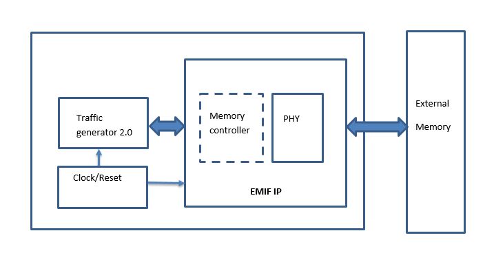
Traffic Generator 2.0 acts as a test vehicle for users to emulate traffic to the external memory, and helps to test, debug and understand the performance of the EMIF Memory interface on their hardware platform in a standalone fashion without having to incorporate their entire design. The Traffic generator2.0 IP (also referred as TG 2.0), offers the ability to customize the testing of the external memory interface as per the user requirements. This offers the user the ability to customize data patterns being written to the memory (PRBS or any user defined pattern), address locations accessed in the memory and the order of write and read transaction patterns. The traffic generator code can be used with any FPGA architecture and memory protocol.
Configuring Traffic Generator 2.0
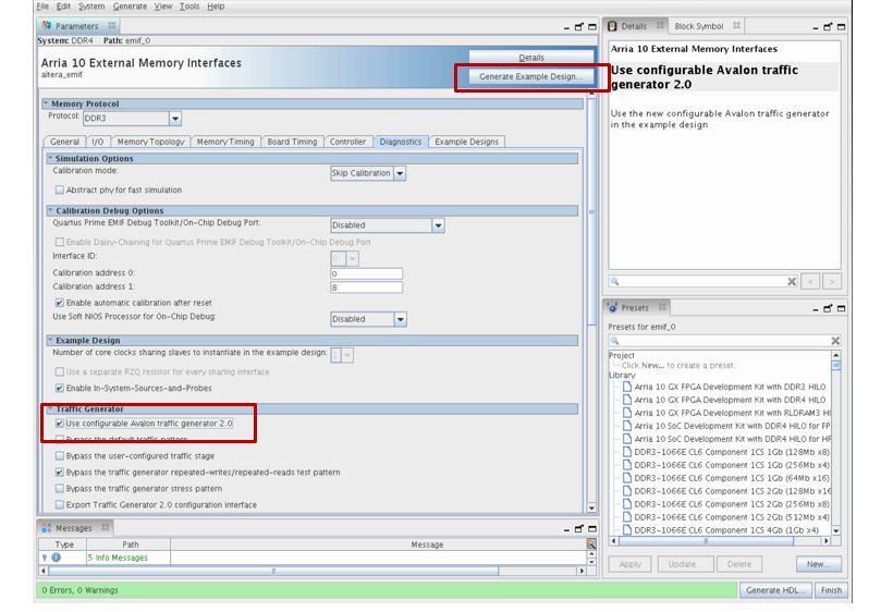
The traffic generator design needs to be incorporated into the EMIF IP design, during the IP generation stage. The traffic generator is intended to replace the user logic that generates the traffic to the external memory. Select the “Generate Example Design” option to generate the Traffic Generator module along with the EMIF IP from the IP Parameter Editor. In the normal operation mode, where the EMIF IP needs to be connected to user logic, use the “Generate HDL” option. If you have an example design with the Traffic Generator 2.0 enabled, you can configure the traffic pattern using the EMIF Debug Toolkit.
Fig1: Traffic Generator 2.0 generated along with EMIF IP in Example Design Mode c/cc/TG20.JPG
To include the Traffic Generator 2.0 design, the user needs to select the following in addition to the Memory and FPGA parameter options in the Diagnostics tab of Qsys:
- Select “Use Configurable Avalon traffic generator 2.0” option to use TG 2.0.
- Select the traffic pattern desired by bypassing the traffic patterns that are not required to be used. The traffic pattern not bypassed will be issued to the memory immediately after calibration is completed. The traffic that can be configured through the EMIF Debug Toolkit, however, can override these patterns.
- Bypass the default traffic pattern - Specifies not to use the default traffic patterns generated by the traffic generator. The default patterns include single read/write, byte-enabled read/write, and block read/write.
- Bypass the user-configured traffic stage - Specifies to skip the stage that uses the user-defined test bench file to configure the traffic generator in simulation. Also enable Export TG 2.0 Configuration interface for this option.
- Bypass the traffic generator repeated-writes/repeated-reads test pattern - Bypasses the traffic generator's repeat test stage, which causes every write and read to be repeated several times.
- Bypass the traffic generator stress pattern - Bypasses a test stage intended to stress test signal integrity and memory interface calibration.
- Export Traffic Generator 2.0 configuration interface - Instantiates a port for traffic generator configuration. Use this port if the traffic generator is to be configured by user logic.
Once the desired parameter options have been selected, click the “Generate Example Design” button at the top of the Parameter Editor. The “Generate Example Design” option enables the generated EMIF IP to include the Traffic Generator 2.0 design with the traffic pattern based on the option selected. It is important to note that selecting the “Generate HDL” option will result in the Traffic Generator 2.0 design not being included.
Fig2: Enabling Traffic Generator 2.0 from IP Parameter Editor 5/59/TG20_fig2.JPG
Running Traffic Generator 2.0 from EMIF Debug Toolkit
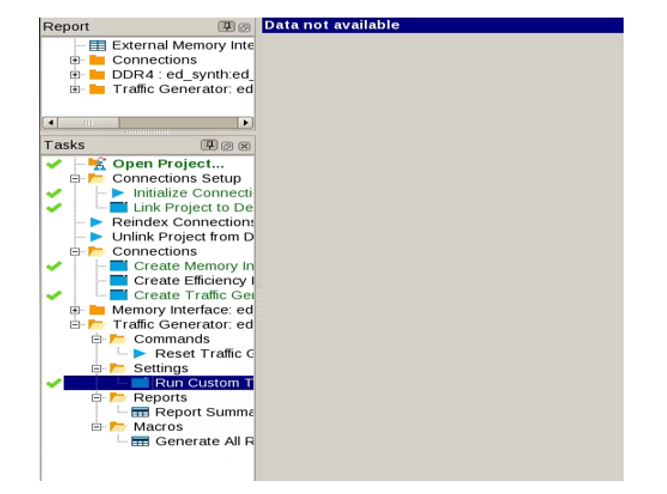
The EMIF Debug Toolkit offers the user interface to take advantage of the underlying Traffic Generator 2.0 infrastructure and to customize traffic patterns to the memory. The EMIF Debug Toolkit can be launched after the FPGA has been programmed.
Once the FPGA has been programmed, launch the EMIF Debug Toolkit from within the Quartus GUI by selecting Tools -> System Debugging Tools -> External Memory Interface Toolkit. After the Toolkit has been launched, the following connections need to be established, prior to running the Custom Traffic Generator.
- Initialize Connections
- Link Project to Device
- Connections
* Create Memory Interface Connection
* Create Traffic Generator Connection
- Now, launch the Traffic Generator from Traffic Generator-> Settings -> Run Custom Traffic pattern. This opens up the window to configure the traffic patterns.
Fig3: Running TG 2.0 from within the EMIF Debug Toolkit 1/11/TG20_fig3.JPG
Custom Traffic Generator GUI
There are three sections available that help the user determine the traffic pattern configuration:
- Data
- Address
- Loops
These tabs help to select the data patterns and the bytes that will be enabled, addressing mode and the order in which the traffic to the memory is organized. The following sections explain each tab in detail.
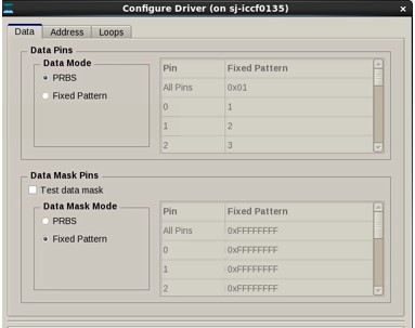
Data Pins
The Data pins section helps with customizing the patterns selected for the data pins.
Data Mode
- PRBS Data pattern is used as the default write data to all the Data pins.
- Fixed Pattern – this option can be used to input a user-specified pattern to be written to the memory. The All Pins option is used when the same data pattern is meant to be written to all the data pins. If data needs to be individually assigned to the data pins, the data value needs to be entered individually into each pin shown in the GUI. The width of the data entered is based on the AVL_TO_DQ_WIDTH_RATIO that is based on the ratio of the memory clock to user clock.
Fig4: Data and Byte enables selection through EMIF Debug Toolkit GUI 0/01/TG20_fig4.jpg
Data Mask Pins
This section allows the user to disable any of the data bytes if desired. All data bytes are enabled by default.
Test data mask - To individually disable the data bytes, select the Test data mask option.
Data Mask Mode
- PRBS – Selecting this option uses the PRBS pattern to enable or disable data bytes. A ‘1’ refers to data byte being enabled and a ‘0’ refers to the data byte being masked or disabled.
- Fixed pattern – Enable or disable each individual byte through this option. The value of the byte enables can be applied on All pins or applied on each individual byte. A ‘1’ refers to data byte being enabled and a ‘0’ refers to the data byte being masked or disabled.
Known issues in “Data” Section
- Fixed pattern option of Data Mode does not work reliably
When the user selects the Fixed Pattern mode in the GUI to enter a specific data pattern, the actual data pattern that gets written to the memory could be different from the value entered through the GUI. For example, when the user enters a write data of all ONEs, the data written to the memory may not be all ONEs. There is an optional workaround for this problem by writing to the internal registers in rtl directly. The instructions to doing this are provided in the section:RTL workaround to reliably write data and enable data bytes
- Required data bytes not enabled as expected
The TG 2.0 design does not enable the correct expected data bytes both in the default mode (all bytes enabled) and when the Test Data mask mode is selected. In the default mode, all data bytes are expected to be enabled. However, the user may not see data written to all bytes as there is a possibility of bytes getting masked. Also, when the Test Data mask option mode is selected, and when select data bytes are disabled, this can also result in the correct bytes not getting disabled. There is an optional workaround for this issue by writing the byte enable values to the internal registers in rtl directly. Refer to the section: RTL workaround to reliably write data and enable data bytes to use this workaround.
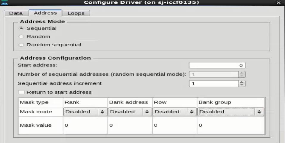
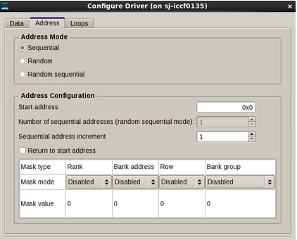
Address
The “Address” tab of the Traffic Generator GUI provides several options to address the memory. The addressing scheme can be sequential, random or random sequential where the initial start address is random but sequential thereafter. The order of operations, including the number of write followed by read transactions, and the number of repeated write or read transactions can be set through the “Loops” tab in the GUI.
Following are the options available through the Address tab:
Address Mode
This specifies the pattern of addresses generated to access the memory:
- Sequential address mode: Each address is incremented by the Sequential address increment. The Start Address specifies the starting address value, while the Sequential Address increment specifies the value by which the addresses increment.
Fig5: Address selection through EMIF Debug Toolkit GUI b/bb/TG20_fig5.png
- Random address mode: Each address is generated randomly. The number of random addresses is set in the “Loops” section.
- Random Sequential address mode: Each address is randomly generated, then incremented sequentially a number of times equal to value in the Number of sequential addresses setting.
Address configuration
- Start address: Defines the starting address value for Sequential Address Mode. The maximum address value that can be reached is 1FF_FFFF. The TG 2.0 GUI, however, does not error while entering a higher value, but wraps around to 0 after the maximum value has reached. This is applicable only to Sequential Address Mode.
- Number of sequential address: Defines the number of sequential addresses generated after the first random address generated. This is used only in the Random Sequential Mode, and not in the Sequential or Random Address Mode.
- Sequential address increment: Defines the size of increment between each address in the Sequential Address Mode and Random Sequential Mode.
- Return to Start Address: Selecting this option enables the address value generated to return back to the value entered in the Start Address tab, after a block of transactions to the memory has completed. This is applicable only to Sequential Mode.
- Address masking: Masking provides additional options to explore certain specific address spaces in the memory. Disabled option does not enable masking, and increments address based on the Address Mode selected. Fixed cycling enables the user to restrict the addressing to either a specific row or bank, which is specified in the corresponding Mask Value. The Full cycling mode helps to explore all the possible address ranges in the specific address configuration enabled.
Known issues with Address generation
- Mask Mode value not retained over successive runs
The default setting on the Address Masking tabs is “Disabled”. However, the Address Masking option changes from a default setting of “Disabled” to “Fixed” while the EMIF Toolkit is opened using the “Start Again” option. This needs to be changed back to “Disabled” again. Setting bank group masking to values other than “Disabled” will lead to design errors in the default setting.
- Supporting bank group masking
When bank group is set to a value other than “Disabled” and sequential or random sequential mode is selected, the Sequential address increment needs to be set to an even number value of 2 or higher. Else the design will error if more than 1 write/read transactions are issued to the memory.
- GUI does not monitor for supported address ranges
The restrictions on the address ranges are not monitored in the Toolkit GUI. The underlying design will wrap the internal address to 0 when the address value exceeds the maximum supported value, however, this is not transparent to the user. It is recommended that the user ensures the address ranges specified in the GUI are within operable ranges.
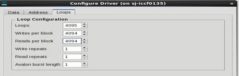
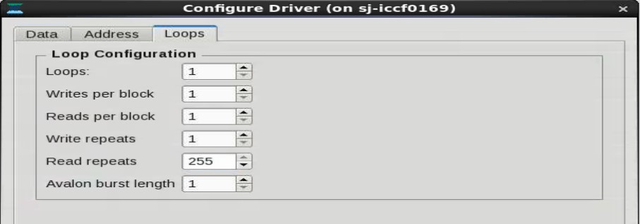
Loops
The “Loops” section helps the user to order the transactions to the memory as desired. A unit size of transactions to the memory is defined as a “block”. This includes a set of write transaction(s) immediately followed by a set of read transaction(s).
Loop configuration:
- Loops: Defines the number of blocks of transactions that are to be executed to the memory. The range of values supported for the number of loops is 1 to 4095. The Loops option helps to extend the range of addresses that the controller can access. The address range is incremented as every loop is executed, unless the “Return to Start Address” is specified, which causes each Loop to start from the same start address.
- Writes per block: This value specifies the size of the block i.e. the number of consecutive write operations that can be issued in a single block. The range of values supported for the number of writes issued in a block are as follows:
- When address masking is disabled, number of writes per block supported is 1 to 4094.
- When address masking is enabled, the max number of writes issued inside a block is 255.
Fig6: Traffic pattern selection through the EMIF Debug Toolkit GUI 6/6d/TG20_fig6.jpg
- Reads per block: This value specifies the number of consecutive read operations that can be issued in a single block, immediately following the consecutive writes issued. The value of number of reads per block should be identical to the number of writes per block, as data mismatches can occur when the two values are not identical. The range of values supported is similar to that of Writes per block.
- Write repeats: This value specifies the number of times each write command is issued in repetition to the same address. A maximum number of 255 repeat write transactions can be issued. The repeat writes are issued immediately after the first write command has been issued.
- Read repeats: This value specifies the number of times each read command is issued in repetition to the same address. A maximum number of 255 repeat read transactions can be issued. The repeat reads are issued immediately after the first read command has been issued.
- Avalon burst length: This value specifies the length of each Avalon burst, and its value should be less than “Sequential Address Increment” value specified in the Address section. The number of write and read repeats default to1 if the Avalon burst length is higher than 1.
Known issues with Loops
- The GUI does not monitor the values entered to be within the supported range. The underlying design will wrap value to 0 when the entered value exceeds the maximum supported value, however, this is not transparent to the user. It is recommended that the user ensures the values specified in the GUI are within operable ranges.
Getting the most out of Traffic Generator 2.0
The traffic generator tool is very useful in running stress tests, debugging the HW platform for Signal Integrity issues in addition to emulating actual memory transactions. Here are some commonly used applications for which the Traffic Generator can come handy.
Using PRBS data pattern for testing Signal integrity
Using PRBS data on the data pins helps to emulate an actual traffic pattern to the memory interface. The Traffic Generator uses PRBS7 data pattern as the default traffic pattern on the data pins, it can support PRBS-15 and PRBS-31.
Single write followed by multiple reads
A single write followed by multiple reads to a specific address can help to debug and monitor a specific address for reliable data capture. This can be set by using the following settings:
- Writes per block -1
- Reads per block – 1
- Write repeats – 1
- Read repeats – 1 to 255
Fig7: Configuring Loops section to support single write followed by multiple reads f/fc/TG20_fig7.jpg
If the “Loops” value is more than 1, every block of WR/multiple RD transactions will follow the same pattern. If there is a specific address to which this transaction needs to be issued, the address can be mentioned in the “Start Address” field in the Address section with Sequential Address Mode selected.
Accessing large sections of the memory
The maximum number of unique addresses that can be written to in one block is limited to 4094. Utilizing the Loops value to the maximum supported value of 4095, the address range that can be supported in one go is (Number of loops * Number of writes per block). Further address expansion can be done by changing the Start Address value appropriately and re-issuing the tests. To continue addressing sections of the memory beyond the address range that can be specified in one set of Toolkit configuration, the Start Address value tab can be used to incrementally access the next set of addresses in the memory. For example, in a memory where row address width is 15, bank address width is 3 and column address width is 10, the total number of address locations to be accessed = 2(row address width) * (bank address width * 2(column address width)). The maximum number of address locations that can be accessed is limited by the width of the internal address bus, that is 25 bits wide.
The following values are required to be set in the Address section for the above case:
- Select Sequential Address mode
- Set Start Address to 0x00
- Ensure Return to Start Address is not selected.
- Make sure address masking for rank, row, bank, bank group is disabled.
Fig8: Address configuration to access the first set of addresses 4/4e/TG20_fig8.jpg
The following values are required to be set in the Loops section:
- Loops – maximum value of 4095
- Writes per block – maximum supported value of 4094
- Reads per block – maximum supported value of 4094
- Write repeats – 1
- Read repeats - 1
Fig9: Loop configuration to access the first set of addresses /e/e7/TG20_fig9.jpg
Each iteration can access a maximum of 4095*4094 locations (16,764,930 address locations i.e. Address ranging from 000_0000’h to FF_D001’h). To access the next 4095*4094 locations the same settings as above need to be repeated, except for Start Address which needs to be set to hex value of 16,764,931 i.e. FF_D002 (see below). The same process can be repeated to further access memory locations inside the memory. The maximum value supported is 25’h 1FF_FFFF which is the equivalent of 33,554,432 locations inside the memory.
Fig10: Address configuration to access the second set of addresses a/a0/TG20_fig10.jpg
RTL workaround to support fixed pattern of data and byte enables
The EMIF Toolkit is designed to provide the user the ability to change write data and to change byte enables from the Toolkit GUI. However, there is an issue, where one or more bytes can end up having incorrect data or byte enable values loaded that can result in unexpected data being written or unexpected bytes being enabled or masked. The workaround here is to manually write the desired data values and byte enable values to the corresponding internal buses in the RTL design itself, prior to compiling the design.
There is also an issue in the Status checker module when the Test data mask option is selected. The design expects masked data bytes to return a value of 1, however, this is not always the case and can result in design errors. The workaround here is to disable the check on the masked bytes.
The workaround is to bypass the GUI interface in the following cases:
- Fixed pattern for data (Same pattern set on All data pins or pattern individually set on Data pins)
- Byte enables – RTL workaround needed when Test data mask option is enabled or disabled.
Two files require modifications, they are traffic_gen and status_checker. The attached files need to replace the existing files in the following directory: project_name/qii/ed_synth/altera_emif_tg_avl_2_160/synth
- altera_emif_avl_tg_2_traffic_gen.sv – This file has to replace the existing file, for reliable operation of the Toolkit. Look for “TG_Updates” and make the necessary changes to update the data and byte enable values.
- altera_emif_avl_tg_2_status_checker.sv – This file has to replace the existing file when data bytes are masked and Test data mask option has been enabled.
The RTL files with the workaround are available in the following page: http://www.alterawiki.com/wiki/Traffic_Generator_2.0:_RTL_workaround_to_support_fixed_pattern_of_Data_and_Byte_enables
Community support is provided during standard business hours (Monday to Friday 7AM - 5PM PST). Other contact methods are available here.
Intel does not verify all solutions, including but not limited to any file transfers that may appear in this community. Accordingly, Intel disclaims all express and implied warranties, including without limitation, the implied warranties of merchantability, fitness for a particular purpose, and non-infringement, as well as any warranty arising from course of performance, course of dealing, or usage in trade.
For more complete information about compiler optimizations, see our Optimization Notice.