- Mark as New
- Bookmark
- Subscribe
- Mute
- Subscribe to RSS Feed
- Permalink
- Report Inappropriate Content
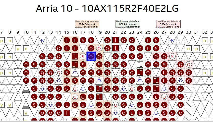
The chip used is 10ax115RF40, and two instances of DDR4 are instantiated, using four banks: 2L, 2K, 3H, and 3G. I used the 2L and 2K DDR4 Fitter successfully, but another DDR4 with 3H and 3G had the following problems. According to Intel's official DDR4 data manual, my Fitter was correct.
Error (14566): The Fitter cannot place 1 periphery component(s) due to conflicts with existing constraints (1 DQ_GRP(s)). Fix the errors described in the submessages, and then rerun the Fitter. The Intel FPGA Knowledge Database may also contain articles with information on how to resolve this periphery placement failure. Review the errors and then visit the Knowledge Database at https://www.altera.com/support/support-resources/knowledge-base/search.html and search for this specific error message number.
Error (175020): The Fitter cannot place logic DQ_GRP that is part of Arria 10 External Memory Interfaces DDR0_altera_emif_180_yyn3hfq in region (142, 196) to (142, 207), to which it is constrained, because there are no valid locations in the region for logic of this type.
Info (14596): Information about the failing component(s):
Info (175028): The DQ_GRP name(s): DDR0:DDR4_A|DDR0_altera_emif_180_yyn3hfq:emif_0|DDR0_altera_emif_arch_nf_180_64hhvbi:arch|DDR0_altera_emif_arch_nf_180_64hhvbi_top:arch_inst|altera_emif_arch_nf_io_tiles_wrap:io_tiles_wrap_inst|altera_emif_arch_nf_io_tiles:io_tiles_inst|tile_gen[0].lane_gen[3].lane_inst_DQ_GRP_1
Error (16234): No legal location could be found out of 2 considered location(s). Reasons why each location could not be used are summarized below:
Error (175005): Could not find a location with: DQ_X9 (2 locations affected)
Info (175029): DQ_GRP containing C19
Info (175029): DQ_GRP containing K17
Info (175015): The I/O pad a_emif_0_mem_mem_dbi_n[0] is constrained to the location PIN_M18 due to: User Location Constraints (PIN_M18)
Info (14709): The constrained I/O pad is contained within a pin, which is contained within this DQ_GRP
Link Copied
- Mark as New
- Bookmark
- Subscribe
- Mute
- Subscribe to RSS Feed
- Permalink
- Report Inappropriate Content
Hello,
Thank you for using Intel Communities.
May I know which Quartus version you are using?
Thanks,
Nurina
- Mark as New
- Bookmark
- Subscribe
- Mute
- Subscribe to RSS Feed
- Permalink
- Report Inappropriate Content
Reassigned to EMIF team.
- Mark as New
- Bookmark
- Subscribe
- Mute
- Subscribe to RSS Feed
- Permalink
- Report Inappropriate Content
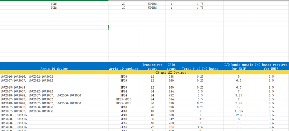
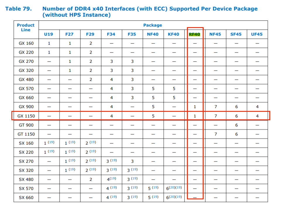
my quartus version is 18.0.Thanks for your reply! I'm new to DDR4. How to realign EMIF GROUP? Is there a tutorial on the official website? Some of the problems I have found are that 10ax115RF40 has a problem with the amount of DDR4 using 40bit data bits, which is 1 on page 200 of a10handbook, but 2 calculated on the emif-device-selector table.
- Mark as New
- Bookmark
- Subscribe
- Mute
- Subscribe to RSS Feed
- Permalink
- Report Inappropriate Content
The number of pins of 3GBANK is 47, and the hard memory controller is not displayed in the software, so can 3G be used as the address and command bank? Since I found that the 3G bank of 10ax115rf40 has no hard memory controller, I would like to ask, so yesterday I used 3H bank as the address and command bank, 3G bank as the data bank, and then similar questions are as follows:
Error (14566): The Fitter cannot place 1 periphery component(s) due to conflicts with existing constraints (1 EMIF_GROUP(s)). Fix the errors described in the submessages, and then rerun the Fitter. The Intel FPGA Knowledge Database may also contain articles with information on how to resolve this periphery placement failure. Review the errors and then visit the Knowledge Database at https://www.altera.com/support/support-resources/knowledge-base/search.html and search for this specific error message number.
Error (175020): The Fitter cannot place logic EMIF_GROUP that is part of Arria 10 External Memory Interfaces DDR0_altera_emif_180_d2i6ggq in region (142, 169) to (142, 207), to which it is constrained, because there are no valid locations in the region for logic of this type.
Info (14596): Information about the failing component(s):
Info (175028): The EMIF_GROUP name(s): EMIF_1_DDR0_altera_emif_180_d2i6ggq
Info (175015): The I/O pad a_emif_0_mem_mem_cs_n[0] is constrained to the location PIN_K20 due to: User Location Constraints (PIN_K20)
Info (14709): The constrained I/O pad is contained within a pin, which is contained within a ADDR_CMD_GRP, which is contained within this EMIF_GROUP
- Mark as New
- Bookmark
- Subscribe
- Mute
- Subscribe to RSS Feed
- Permalink
- Report Inappropriate Content
@niceflower wrote:
The number of pins of 3GBANK is 47, and the hard memory controller is not displayed in the software, so can 3G be used as the address and command bank? Since I found that the 3G bank of 10ax115rf40 has no hard memory controller, I would like to ask, so yesterday I used 3H bank as the address and command bank, 3G bank as the data bank, and then similar questions are as follows:
Error (14566): The Fitter cannot place 1 periphery component(s) due to conflicts with existing constraints (1 EMIF_GROUP(s)). Fix the errors described in the submessages, and then rerun the Fitter. The Intel FPGA Knowledge Database may also contain articles with information on how to resolve this periphery placement failure. Review the errors and then visit the Knowledge Database at https://www.altera.com/support/support-resources/knowledge-base/search.html and search for this specific error message number.
Error (175020): The Fitter cannot place logic EMIF_GROUP that is part of Arria 10 External Memory Interfaces DDR0_altera_emif_180_d2i6ggq in region (142, 169) to (142, 207), to which it is constrained, because there are no valid locations in the region for logic of this type.
Info (14596): Information about the failing component(s):
Info (175028): The EMIF_GROUP name(s): EMIF_1_DDR0_altera_emif_180_d2i6ggq
Info (175015): The I/O pad a_emif_0_mem_mem_cs_n[0] is constrained to the location PIN_K20 due to: User Location Constraints (PIN_K20)
Info (14709): The constrained I/O pad is contained within a pin, which is contained within a ADDR_CMD_GRP, which is contained within this EMIF_GROUP
How to realign EMIF GROUP? Is there a tutorial on the official website? Some of the problems I have found are that 10ax115RF40 has a problem with the amount of DDR4 using 40bit data bits, which is 1 on page 200 of a10handbook, but 2 calculated on the emif-device-selector table.
- Mark as New
- Bookmark
- Subscribe
- Mute
- Subscribe to RSS Feed
- Permalink
- Report Inappropriate Content
Hi,
The IO Bank 2L,2K and IO Bank 3H,3G are not located in a same IO Column.
There is no connection in between the IO Columns.
Please choose the IO Banks that located in a same IO Columns if the interfaces are connecting to each other.
Regards,
Adzim
- Mark as New
- Bookmark
- Subscribe
- Mute
- Subscribe to RSS Feed
- Permalink
- Report Inappropriate Content
I know it.I am instantiating two DDR4 instances, one of which is successfully instantiated (2L, 2K) and the other is not successfully instantiated (3H, 3G), which is not ping-pong PHY.
- Mark as New
- Bookmark
- Subscribe
- Mute
- Subscribe to RSS Feed
- Permalink
- Report Inappropriate Content
Hi,
I have checked the IO Bank 3G that has 47 pins. The pins at index 1-11 are not able to be used for DQ/DQS signal.
Then the second EMIF interface need to disable ECC so that the DQ width can set to 32 to fit into this IO bank.
If you cannot do so, you may choose another IO Bank such IO Bank 2A and 2F.
I have attached your design that can be fitted in IO Bank 3G and 3H. But the DQ width is set to 32.
Regards,
Adzim
- Mark as New
- Bookmark
- Subscribe
- Mute
- Subscribe to RSS Feed
- Permalink
- Report Inappropriate Content
As we do not receive any response from you on the previous reply that we have provided, I now transition this thread to community support. Please login to ‘https://supporttickets.intel.com’, view details of the desire request, and post a feed/response within the next 15 days to allow me to continue to support you. After 15 days, this thread will be transitioned to community support. The community users will be able to help you on your follow-up questions.
- Subscribe to RSS Feed
- Mark Topic as New
- Mark Topic as Read
- Float this Topic for Current User
- Bookmark
- Subscribe
- Printer Friendly Page


