- Mark as New
- Bookmark
- Subscribe
- Mute
- Subscribe to RSS Feed
- Permalink
- Report Inappropriate Content
Most of the signals relate to NIOS. The design based on a single 100MHz clock. There is an additional clock 12.5MHz generated in pll in QSYS and connected only to epcs flash controller. I've seen similar connection of the epcs flash controller in some examples.
I get no setup time violations and functionally everything works fine. But I can't get rid of hold time violation warnings. See the attached TimeQuest Report. Please help.
Thank you.

Link Copied
- Mark as New
- Bookmark
- Subscribe
- Mute
- Subscribe to RSS Feed
- Permalink
- Report Inappropriate Content
A few things: 1) for a hold analysis, you should be looking at the fast timing model. 2) Your report_timing command is looking at all paths latched by clk[0]. Is this what you intend to look at? I would want to see you scroll down in that data path tab to try to figure out why the from and to nodes are the same. I would also want to see your .sdc, and your clock and clock summary reports. It's hard to diagnose with what you have here.
- Mark as New
- Bookmark
- Subscribe
- Mute
- Subscribe to RSS Feed
- Permalink
- Report Inappropriate Content
One way to resolve Hold issues, is to phase shift your clock. If the design uses a PLL, then you can phase shift the clock by a few degrees and see if the hold violations are resolved. I had a similar kind of issue with Hold violations in my Qsys design. I then shifted the generated clocks by 90 and re-compiled and the hold violations were gone, did see a better slack margin as well as Fmax of the design also went up.
- Mark as New
- Bookmark
- Subscribe
- Mute
- Subscribe to RSS Feed
- Permalink
- Report Inappropriate Content
Thank you @sstrell ,
- Sure, I get this warnings for fast as well as for slow models.
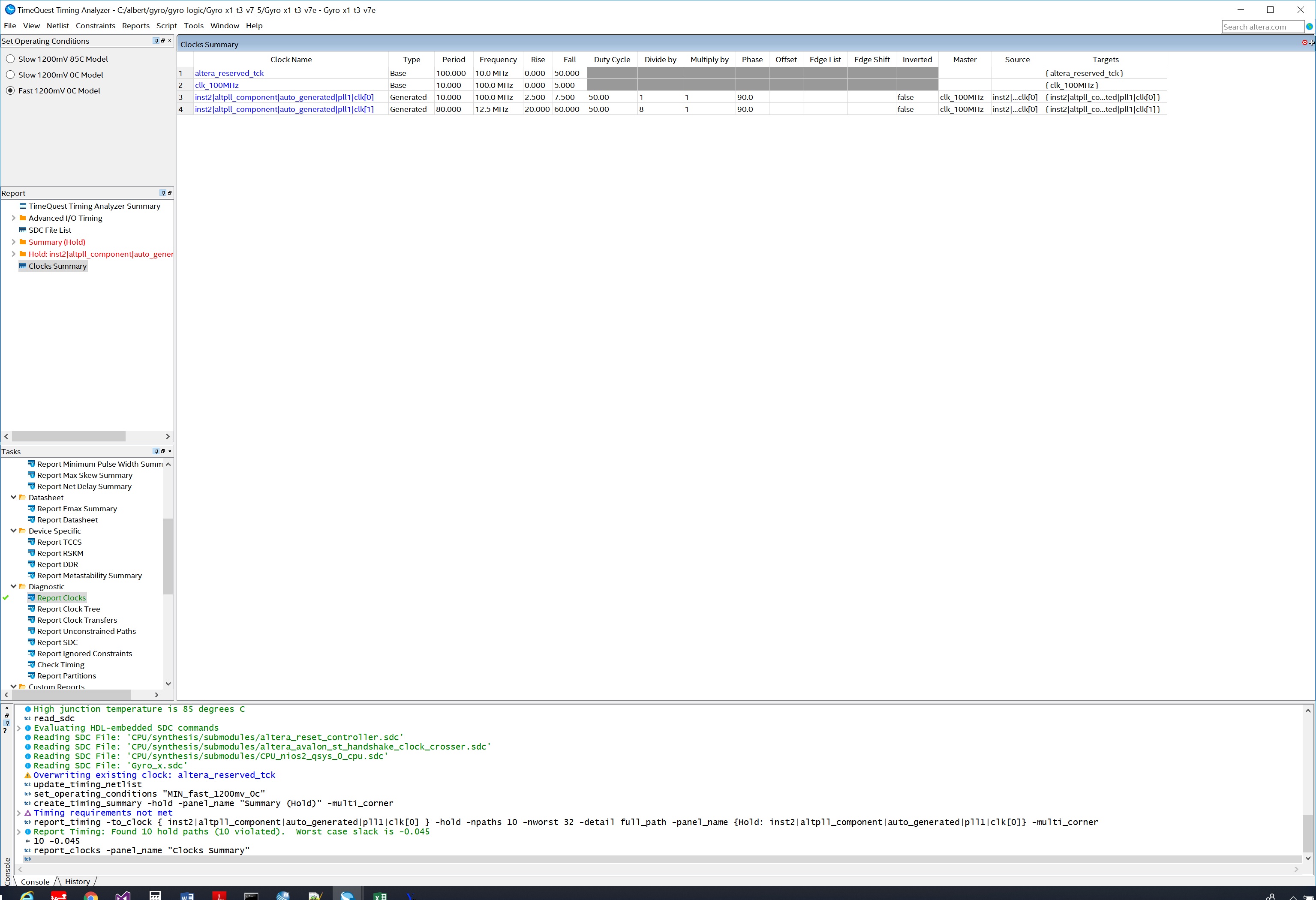
- Yes, clk[0] is my system clock. See attached scrolled down of the data arrival and the data required paths, the .sdc file and the clock report.
Thank you!
- Mark as New
- Bookmark
- Subscribe
- Mute
- Subscribe to RSS Feed
- Permalink
- Report Inappropriate Content
- Mark as New
- Bookmark
- Subscribe
- Mute
- Subscribe to RSS Feed
- Permalink
- Report Inappropriate Content
- Mark as New
- Bookmark
- Subscribe
- Mute
- Subscribe to RSS Feed
- Permalink
- Report Inappropriate Content
- Mark as New
- Bookmark
- Subscribe
- Mute
- Subscribe to RSS Feed
- Permalink
- Report Inappropriate Content
Thank you @Abe , I just have tried to change the phase by 90 deg., got a different result, but the hold warnings still here... I'll try different phases.
I don't really expect to see hold violations, there is a problem here and I can't figure out what could it be.
Thank you.
- Mark as New
- Bookmark
- Subscribe
- Mute
- Subscribe to RSS Feed
- Permalink
- Report Inappropriate Content
Assuming the 100 MHz clock is driving the "upstream" and "downstream" devices this FPGA is connected to, you should have a separate virtual clock constraint and reference it in you set_input[output]_delay constraints and use derive_clock_uncertainty to get the most accurate uncertainties on I/O:
create_clock -name clock_in_vir -period 10
create_clock -name clock_out_vir -period 10
set_input_delay -clock clock_in_vir ...
set_output_delay -clock clock_out_vir ...
Aside from that, looking at the timing reports, these failures seem to be feedback loops in your design. I'm not sure why you have such loops, but it might be useful to look back at your code to try to understand them. You can cross-probe from the timing reports by right-clicking a failing timing path and select Locate Path. It might be helpful to see these paths in the Technology Map Viewer to understand what they're connected through and what they're doing.
- Mark as New
- Bookmark
- Subscribe
- Mute
- Subscribe to RSS Feed
- Permalink
- Report Inappropriate Content
Thank you @sstrell , I'm updating the .sdc file.
I checked the paths with the Technology Map and the failures really caused by feedback loops. But these loops are in different Altera's IPs code - FIFO, EPCS controller so it is not clear what they are doing exactly...
I'll try to understand better what happens.
Thank you for your help.
- Mark as New
- Bookmark
- Subscribe
- Mute
- Subscribe to RSS Feed
- Permalink
- Report Inappropriate Content
Hi ACoga,
Have you try to add delay in the path?
Thanks.
- Mark as New
- Bookmark
- Subscribe
- Mute
- Subscribe to RSS Feed
- Permalink
- Report Inappropriate Content
Hi @KhaiY_Intel ,
No, most of the warnings relate to Altera IP code such as FIFO, EPCS controller, NIOS, so I can't change the design.
Thank you.
- Mark as New
- Bookmark
- Subscribe
- Mute
- Subscribe to RSS Feed
- Permalink
- Report Inappropriate Content
Hi Hi ACoga,
Do you mind to share the design?
Thanks
- Mark as New
- Bookmark
- Subscribe
- Mute
- Subscribe to RSS Feed
- Permalink
- Report Inappropriate Content
It's possible. How can I do it?
- Mark as New
- Bookmark
- Subscribe
- Mute
- Subscribe to RSS Feed
- Permalink
- Report Inappropriate Content
- Mark as New
- Bookmark
- Subscribe
- Mute
- Subscribe to RSS Feed
- Permalink
- Report Inappropriate Content
- Mark as New
- Bookmark
- Subscribe
- Mute
- Subscribe to RSS Feed
- Permalink
- Report Inappropriate Content
Hi YY,
Unfortunately, I have restrictions to share the design...
Do you have any ideas what can I check to get rid of these warnings?
Thank you.
- Mark as New
- Bookmark
- Subscribe
- Mute
- Subscribe to RSS Feed
- Permalink
- Report Inappropriate Content
- Mark as New
- Bookmark
- Subscribe
- Mute
- Subscribe to RSS Feed
- Permalink
- Report Inappropriate Content
Thank you very much @KhaiY_Intel , great explanations. I'll try to overconstrain, but it looks that I have a problem with some settings. The warnings don't look real - all of them from and to the same node...
- Mark as New
- Bookmark
- Subscribe
- Mute
- Subscribe to RSS Feed
- Permalink
- Report Inappropriate Content
- Mark as New
- Bookmark
- Subscribe
- Mute
- Subscribe to RSS Feed
- Permalink
- Report Inappropriate Content
Hi @KhaiY_Intel ,
I haven't solved it yet. Not really clear how to overconstrain the hold warnings of the same clock To and From the same signal. The number of the warnings (I could see a few hundreds of them and don't know the exact number - could be much higher) makes me think that something basic is wrong.
I've tried to remove the .sdc file and leave only derive_pll_clocks, but this type of warnings still appears, so it is not the .sdc file issue.
I'm working with Quartus 16.1, someone advised me to try a newer version. I can try it on the next week.
If you have any new ideas, I'll appreciate it.
Thank you.
- Subscribe to RSS Feed
- Mark Topic as New
- Mark Topic as Read
- Float this Topic for Current User
- Bookmark
- Subscribe
- Printer Friendly Page