- Mark as New
- Bookmark
- Subscribe
- Mute
- Subscribe to RSS Feed
- Permalink
- Report Inappropriate Content
Clearly i'm a newbie, but I'm really stuck with what is I'm sure a simple problem.
I am using a .bdf to code a Cyclone IV FPGA using Quartus Lite v18.
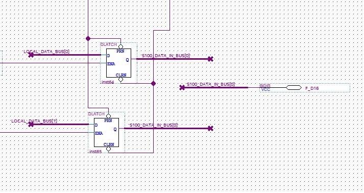
I have a circuit with an "internal" 8 bit data bus which I need to bring out to 8 FPGA bidirectional pins. If I draw for example DATA_BUS[0] connected to a BDIR pin no problem. However if I connect another gate to this DATA_BUS[0] I get an error saying DATA_BUS[0] can only be assigned one value. I thought the use of a data bus is that various gates can interface with it. The actual interface is a data latch with its one ENA.
How does one get around this. I tried all kinds of approaches. The only thing that worked was a MUX with two outputs. I attaching a simple example here
Link Copied
- Mark as New
- Bookmark
- Subscribe
- Mute
- Subscribe to RSS Feed
- Permalink
- Report Inappropriate Content
Hello JMona1,
Pins on an FPGA have special logic to implement inout behaviour.
They can have high impedance (Hi-Z) or output.
Signals on internal FPGA logic (your flipflops) do not have this logic.
What you are trying to do is to have 2 flipflops control 1 fpga pin.
If the state of flipflop A is 1 and the B is 0, then what should the value of the pin be?
So this is the reason if you connect 1 flipflop with a pin, you are ok, if you connect 2 flipflop outputs to 1 fpga pin, you are in trouble.
Mux is a good solution, you can use other solutions a logic OR of both signals provided you can guarantee all are 0 except one. This is a kind of "open collector" hardware approach equivalent.
If you implement a cpu in an FPGA (Nios-II) for example, you will see that PIO signals that are configured in platform designer as inout end up as a single in and a single out port. Signals that are ment to control SDRAM dual port pins end up as inout signals.
There could be other solutions as well, but I do not consider my self an expert in the matter.
Best Regards,
Johi.
- Mark as New
- Bookmark
- Subscribe
- Mute
- Subscribe to RSS Feed
- Permalink
- Report Inappropriate Content
Thanks Johi, I understand what you have there but thought there was another way and I was overlooking something. Wish the was the equivalent of an Open Collector gate is these FPGA's.
I don't however understand why I cannot use Output enables OE*. Say using the 74244's. If they behave like the 'real' 74244s, multiple gates should not affect an output pin function if only one is active at a time. Why does that not work -- be accepted by Quartus.
- Subscribe to RSS Feed
- Mark Topic as New
- Mark Topic as Read
- Float this Topic for Current User
- Bookmark
- Subscribe
- Printer Friendly Page