- Mark as New
- Bookmark
- Subscribe
- Mute
- Subscribe to RSS Feed
- Permalink
- Report Inappropriate Content
Hello,
I've been trying to validate my pin assignment for an FPGA design that I am working on. I have LVDS inputs and outputs in my design.
I have problems with assigning LVDS pins.
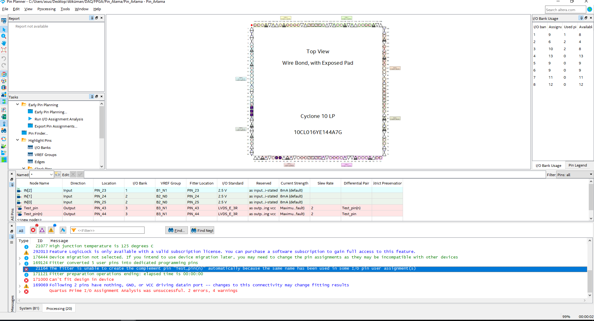
Whenever I try to assign LVDS pin I get this error : "Error (21164): The fitter is unable to create the complement pin "Test_pin(n)" automatically because the same name has been used in some I/O pin user assignment(s)". This spesifically happens when I set the direction of the LVDS pin. When I leave the direction area empty I don't get any errors.
How can I solve this problem?
Thanks!
- Tags:
- lvds
- Mark as New
- Bookmark
- Subscribe
- Mute
- Subscribe to RSS Feed
- Permalink
- Report Inappropriate Content
I don't know what logic you have in the module, but I have done a simple design just to show you how to assign the LVDS pins for the same device. When assigning pins , you need to keep in mind the IO Standard, voltage as well as the IO Type (Single-function, clock output, dual-purpose, etc).
This is the code I used for the sample build:
module c10_lvds(
	input wire  [2:0] In,
	output wire [2:0] Test_pin
	);

	wire [2:0]  core_input;
	wire            lvds_clock;

	ALT_INBUF inbuf0 (
	                  .i( In[0]         ),
	                  .o( core_input[0] )
					);

	ALT_INBUF inbuf1 (
	                  .i( In[1]         ),
	                  .o( core_input[1] )
					);

	ALT_INBUF inbuf2 (
	                  .i( In[2]         ),
	                  .o( core_input[2] )
			);


   // Have to include PLL since PIN_43/44 are Differential Clock outputs
   // Need to be driven by output clocks from PLL.

	lvds_pll_out	lvds_pll_inst (
	                              .inclk0 ( core_input[0] ),
	                              .c0 ( lvds_clock )
	                             );

	ALT_OUTBUF outbuff0_lvds (
	                         .i( lvds_clock ),
				 .o( Test_pin[0]   )
				 );

	// Since these IO are normal IO, these can be driven by any signal
	// PLL outputs need not be used for these IO
	ALT_OUTBUF outbuff1_lvds (
	                         .i( core_input[1] ),
				 .o( Test_pin[1]   )
				 );


	ALT_OUTBUF outbuff2_lvds (
	                         .i( core_input[2] ),
				 .o( Test_pin[2]   )
				 );

endmodule
I assigned the pins using Assignment Editor after compiling the design. The direction gets assigned automatically based on the design. You can see the assignments made in the Assignment Editor as well as Pin Planner:


Link Copied
- Mark as New
- Bookmark
- Subscribe
- Mute
- Subscribe to RSS Feed
- Permalink
- Report Inappropriate Content
When assigning LVDS pins, you only need assign the +ve (p) pin to the correct _p pin in the device and set the IO Standard as LVDS. The tool will automatically assign the compliment -ve (n) pin for that LVDS pin. What you need to do is just delete the Test_pin(n) assignment you made and leave only the Test_pin assigned to the corresponding LVDS +ve (p) pin (PIN_43) and then compile the design. This will solve the issue for you.
- Mark as New
- Bookmark
- Subscribe
- Mute
- Subscribe to RSS Feed
- Permalink
- Report Inappropriate Content
Thanks for your response Abe,
Could you also tell me how to set the direction (Input, output). When I set the direction from the reserved column it gives me the same error.
Thanks.
- Mark as New
- Bookmark
- Subscribe
- Mute
- Subscribe to RSS Feed
- Permalink
- Report Inappropriate Content
I don't know what logic you have in the module, but I have done a simple design just to show you how to assign the LVDS pins for the same device. When assigning pins , you need to keep in mind the IO Standard, voltage as well as the IO Type (Single-function, clock output, dual-purpose, etc).
This is the code I used for the sample build:
module c10_lvds(
	input wire  [2:0] In,
	output wire [2:0] Test_pin
	);

	wire [2:0]  core_input;
	wire            lvds_clock;

	ALT_INBUF inbuf0 (
	                  .i( In[0]         ),
	                  .o( core_input[0] )
					);

	ALT_INBUF inbuf1 (
	                  .i( In[1]         ),
	                  .o( core_input[1] )
					);

	ALT_INBUF inbuf2 (
	                  .i( In[2]         ),
	                  .o( core_input[2] )
			);


   // Have to include PLL since PIN_43/44 are Differential Clock outputs
   // Need to be driven by output clocks from PLL.

	lvds_pll_out	lvds_pll_inst (
	                              .inclk0 ( core_input[0] ),
	                              .c0 ( lvds_clock )
	                             );

	ALT_OUTBUF outbuff0_lvds (
	                         .i( lvds_clock ),
				 .o( Test_pin[0]   )
				 );

	// Since these IO are normal IO, these can be driven by any signal
	// PLL outputs need not be used for these IO
	ALT_OUTBUF outbuff1_lvds (
	                         .i( core_input[1] ),
				 .o( Test_pin[1]   )
				 );


	ALT_OUTBUF outbuff2_lvds (
	                         .i( core_input[2] ),
				 .o( Test_pin[2]   )
				 );

endmodule
I assigned the pins using Assignment Editor after compiling the design. The direction gets assigned automatically based on the design. You can see the assignments made in the Assignment Editor as well as Pin Planner:
- Mark as New
- Bookmark
- Subscribe
- Mute
- Subscribe to RSS Feed
- Permalink
- Report Inappropriate Content
- Subscribe to RSS Feed
- Mark Topic as New
- Mark Topic as Read
- Float this Topic for Current User
- Bookmark
- Subscribe
- Printer Friendly Page