- Mark as New
- Bookmark
- Subscribe
- Mute
- Subscribe to RSS Feed
- Permalink
- Report Inappropriate Content
Hey everyone
I'm at the very beginning of a project where I want to implement a power converter digital controller on a MAX10 device. I have a little experience, but only with Lattice FPGAs and tools.
I'm using the MAX1000 development board with a 10M08SAU169C8G and Quartus Prime 20.1.
As a start I've implemented a binary counter using the on-board 12MHz oscillator and 8 LEDs. It works but I get the following warning, that I would like to handle:
Info (169124): Fitter converted 4 user pins into dedicated programming pins
Info (169125): Pin ~ALTERA_TMS~ is reserved at location G1
Info (169125): Pin ~ALTERA_TCK~ is reserved at location G2
Info (169125): Pin ~ALTERA_TDI~ is reserved at location F5
Info (169125): Pin ~ALTERA_TDO~ is reserved at location F6
Info (169141): DATA[0] dual-purpose pin not reserved
Info (12825): Data[1]/ASDO dual-purpose pin not reserved
Info (12825): nCSO dual-purpose pin not reserved
Info (12825): DCLK dual-purpose pin not reserved
Warning (15714): Some pins have incomplete I/O assignments. Refer to the I/O Assignment Warnings report for details
Seems it first complains about the JTAG pins, but after that about another (or the same?) 4 dual-purpose pins.
Does anybody know what I'm supposed to do here?
Also there is a warning, that I didn't specify timing constraints:
Critical Warning (332012): Synopsys Design Constraints File file not found: 'counter.sdc'. A Synopsys Design Constraints File is required by the Timing Analyzer to get proper timing constraints. Without it, the Compiler will not properly optimize the design.
Can somebody point me to a tutorial for a starting point how to do this?
Many thanks and all the best
Gaston
Link Copied
- Mark as New
- Bookmark
- Subscribe
- Mute
- Subscribe to RSS Feed
- Permalink
- Report Inappropriate Content
Hello,
meassage lines starting with "info" are no warnings, just processing information. The warning about incomplete I/O assignments can be traced in the Fitter report/Resource Section/I/O Standards Section/I/O Assignments Warnings. You'll find hints like missing drive strength or missing location assignment for specific pins.
You should have a .sdc file that at least declares the pin and frequency of your clock input. This enables the timing analyser to check the internal timing of your design.
Frank
- Mark as New
- Bookmark
- Subscribe
- Mute
- Subscribe to RSS Feed
- Permalink
- Report Inappropriate Content
This is what I find in the I/O Assignment Warnings:
This is the list in pin planner:
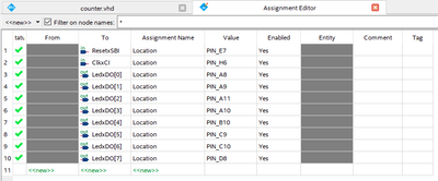
The assignment editor:
And the top vhdl:
library ieee;
use ieee.std_logic_1164.all;
use ieee.numeric_std.all;
use work.Counter_pack.all;

entity counter is

 	port (

	ResetxSBI    		: in  std_logic;
	ClkxCI      		: in  std_logic;
   LedxDO     			: out std_logic_vector(7 downto 0)

	);

end counter;


architecture behavioral of counter is

	signal CountValuexD						    : unsigned(COUNTER_WIDTH-1 downto 0); -- count value

begin

	CntStateMachine: process (ClkxCI,ResetxSBI)
	begin
		if ResetxSBI = '0' then

			CountValuexD <= to_unsigned(0,COUNTER_WIDTH);

		elsif ClkxCI'event and ClkxCI = '1' then

			-- determine next counter value
			CountValuexD <= CountValuexD + to_unsigned(1,COUNTER_WIDTH);

		end if;
	end process CntStateMachine;

	-- assign outputs
	LedxDO <= std_logic_vector(CountValuexD(COUNTER_WIDTH-1 downto COUNTER_WIDTH-8));


end behavioral;
The mesage incomplete set of assignments seems to refer to the only two inputs of the design. The outputs seem to be OK. But I don't understand what's missing.
- Mark as New
- Bookmark
- Subscribe
- Mute
- Subscribe to RSS Feed
- Permalink
- Report Inappropriate Content
clk_clk and reset_reset_n don't even appear in your design. Do you have any idea where these are coming from?
- Mark as New
- Bookmark
- Subscribe
- Mute
- Subscribe to RSS Feed
- Permalink
- Report Inappropriate Content
Hi,
Do you still the warning massage in the I/O Assignment Warnings?
- Subscribe to RSS Feed
- Mark Topic as New
- Mark Topic as Read
- Float this Topic for Current User
- Bookmark
- Subscribe
- Printer Friendly Page


