- Mark as New
- Bookmark
- Subscribe
- Mute
- Subscribe to RSS Feed
- Permalink
- Report Inappropriate Content
Hi,
I have a question concerning a warning that I get when compiling my design. The warning is as follows: Warning: PLL "pll_for_fft:inst28|altpll:altpll_component|pll_for_fft_altpll:auto_generated|pll1" input clock inclk[0] is not fully compensated and may have reduced jitter performance because it is fed by a non-dedicated input So as far as I understand the meaning of this warning, it says that the signal that is fed into the PLL (which in this case comes directly from a physical I/O pin of the FPGA) is not a dedicated clock signal. Well, in my understanding, the input pin from where that signal is routed IS a dedicated clock (input) pin. Is that so (please see attachment)? Or where can I find a dedicated clock input pin that would make this warning go away? Thanks, Maik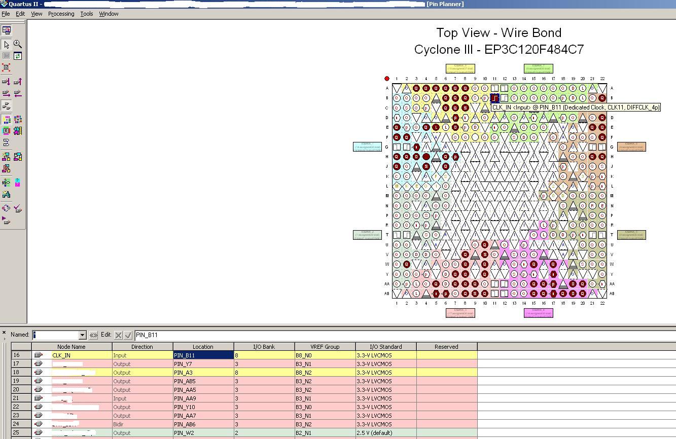
Link Copied
6 Replies
- Mark as New
- Bookmark
- Subscribe
- Mute
- Subscribe to RSS Feed
- Permalink
- Report Inappropriate Content
--- Quote Start --- Hi, I have a question concerning a warning that I get when compiling my design. The warning is as follows: Warning: PLL "pll_for_fft:inst28|altpll:altpll_component|pll_for_fft_altpll:auto_generated|pll1" input clock inclk[0] is not fully compensated and may have reduced jitter performance because it is fed by a non-dedicated input So as far as I understand the meaning of this warning, it says that the signal that is fed into the PLL (which in this case comes directly from a physical I/O pin of the FPGA) is not a dedicated clock signal. Well, in my understanding, the input pin from where that signal is routed IS a dedicated clock (input) pin. Is that so (please see attachment)? Or where can I find a dedicated clock input pin that would make this warning go away? Thanks, Maik --- Quote End --- Does your clock pin feed the PLL directly and exclusively. I mean do you use same clock for some other sections?
- Mark as New
- Bookmark
- Subscribe
- Mute
- Subscribe to RSS Feed
- Permalink
- Report Inappropriate Content
I use the pin for another PLL . . . .
- Mark as New
- Bookmark
- Subscribe
- Mute
- Subscribe to RSS Feed
- Permalink
- Report Inappropriate Content
Hi kaz,
to answer a little bit more detailed: I have this one clock in pin available and connect it directly to 2 PLLs. In my Design I have several different clock rates. So I decided to use the avilable PLLs in order to make the Timing analysis easier by just using "derive_pll_clocks -create_base_clocks" in my sdc file. Now, I see that it was not meant to conneckt more than 1 PLL to a dedicated clock input pin, is that right? So I guess I have to generate just a subset of my needed clock rates and use clock enables to get the rest of my system be clocked as needed. I cannot change the hardware anymore since this development is long finished . . . Regards, Maik- Mark as New
- Bookmark
- Subscribe
- Mute
- Subscribe to RSS Feed
- Permalink
- Report Inappropriate Content
I think some clock pins can feed more than one PLL, but I don't know Cyclone III very well. Try consulting the Cyclone III device handbook, it should have a diagram showing which dedicated clock pins can feed which physical PLLs.
- Mark as New
- Bookmark
- Subscribe
- Mute
- Subscribe to RSS Feed
- Permalink
- Report Inappropriate Content
Hi aludwin,
thanks, I found a table that shows how many global clock networks can be drivven by an input pin. I guess that's it. Thank you for the information. Maik- Mark as New
- Bookmark
- Subscribe
- Mute
- Subscribe to RSS Feed
- Permalink
- Report Inappropriate Content
I had a similar problem, because my input clock was marked as a global clock.
Removing this from my .qsf file solved the issue:
set_instance_assignment -name GLOBAL_SIGNAL "GLOBAL CLOCK" -to clk
Reply
Topic Options
- Subscribe to RSS Feed
- Mark Topic as New
- Mark Topic as Read
- Float this Topic for Current User
- Bookmark
- Subscribe
- Printer Friendly Page