- Mark as New
- Bookmark
- Subscribe
- Mute
- Subscribe to RSS Feed
- Permalink
- Report Inappropriate Content
Hi,
What I want to do is loan the GPIO 57~60 on the cyclone V soc board to the FPGA,
these four pins act as SPIM0-CLK, SPIM0-MOSI, SPIM0-MISO and SPIM0-SS0.
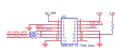
And these pins are connected to J32 pin SCK, MOSI, MISO and CSn.
Now I have a device connected to these four pins on J32 physically.
Right now can I control these pins on FPGA ?
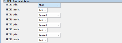
What's the difference between loan IO to FPGA and set the SPI to FPGA in HPS design directly?
Unuse the pin and loan the io
Set to FPGA directly
Physical connection to J32
Reguards.
Link Copied
- Mark as New
- Bookmark
- Subscribe
- Mute
- Subscribe to RSS Feed
- Permalink
- Report Inappropriate Content
Loan I/O means that the pins would not be used for SPI from the HPS anymore. They would be available in the Quartus Pin Planner for you to connect signals from the FPGA side of the device.
It looks like choosing FPGA gives you these connections to the SPI controller: https://www.intel.com/content/www/us/en/docs/programmable/683126/21-2/fpga-routing-61665.html
- Mark as New
- Bookmark
- Subscribe
- Mute
- Subscribe to RSS Feed
- Permalink
- Report Inappropriate Content
Hi,
Thank you for your answer and wiling to help.
Do you know if I can control these four pins (MISO,MOSI,SCK_SCL and CSn) through FPGA ?
Another question is, when I set the pins as LoanIO, and use the inout wire to link to them in top design file, I got the following error:
Error (169026): Pin hps_gpio_loan57 with I/O standard assignment 2.5 V is incompatible with I/O bank 7A. I/O standard 2.5 V, has a VCCIO requirement of 2.5V, which incompatible with the I/O bank's VCCIO setting or with other output or bidirectional pins in the I/O bank using a VCCIO requirement of 3.3V. Assign output and bidirectional pins with different VCCIO requirements to different I/O banks, or change the I/O standard assignment for the specified pin to a compatible I/O standard. The Intel FPGA Knowledge Database contains many articles with specific details on how to resolve this error. Visit the Knowledge Database at https://www.altera.com/support/support-resources/knowledge-base/search.html and search for this specific error message number.
The default setting of these loan IO is 2.5 V BTW.
Reguards.
- Mark as New
- Bookmark
- Subscribe
- Mute
- Subscribe to RSS Feed
- Permalink
- Report Inappropriate Content
As the error says, you have other pins in the I/O bank that are set to 3.3 V instead of 2.5V. You either need to change their voltage or move them to different locations in a different I/O bank.
- Mark as New
- Bookmark
- Subscribe
- Mute
- Subscribe to RSS Feed
- Permalink
- Report Inappropriate Content
Hi,
I've already set the GPIO 58 and 59 as loan IO, and export the IOs.
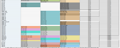
Mux Table setting
Pin planner setting
By using the Loan IO 58 and 59, I set the 58 as in and linked to my other RS232 module RXD and 59 as out linked to TXD.
top level setting 1
top level setting 2
As mentioned by Accessing HPS Devices from the FPGA (intel.com) chap 2.2,
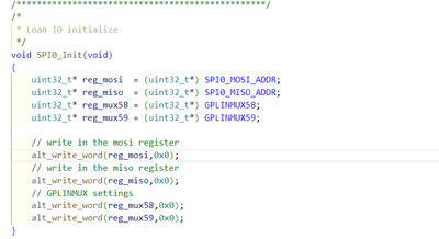
In HPS baremetal code I set the GENERALIO_10/11 and GPLINMUX58/59 to 0x0
HPS baremetal settings
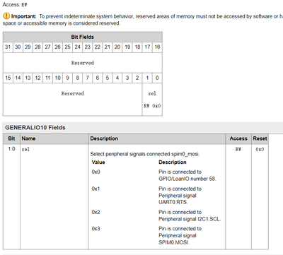
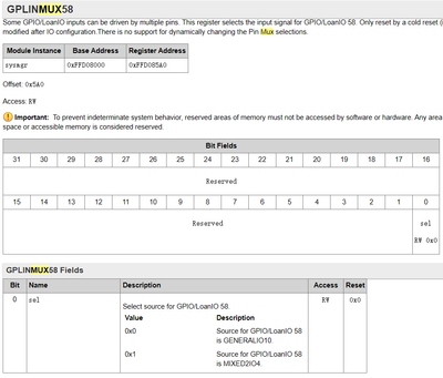
According to Cyclone V HPS Register Address Map and Definitions - GENERALIO10 (intel.com)
(For example general IO 10 and MUX58)
general IO 10
MUX 58
The pin is linked to Genral IO 10 as a loan IO 58.
After doing that I checked the value of these registers
their low 2 bits are =2'b00
And in FPGA board I sent the signal to the pin loan_io_out_59 but I didnt receive any signal from that pin.
Did I do something wrong with that?
What's the right steps to deal with loanIO under baremetal environment?
Reguards.
- Mark as New
- Bookmark
- Subscribe
- Mute
- Subscribe to RSS Feed
- Permalink
- Report Inappropriate Content
Also, I've been checking the HPS reference book:
"Each LoanIO port has an input, output, and output enable, which directly controls the HPS IO functions.
The LoanIO only operates when the HPS registers have been set up in the pre-loader to allow their
operation. The LoanIO are asynchronous, thus no clocking is required."
So what is the necessary setting of the pre-loader? and HOW?
- Mark as New
- Bookmark
- Subscribe
- Mute
- Subscribe to RSS Feed
- Permalink
- Report Inappropriate Content
Now Im totally confused by the directions:
I have three parts:
hardware IO : HTX , HRX.
software IO :STX,SRX.
generally HTX -> SRX , HRX <- STX.
Now I borrowed the HPS IO to the FPGA, they are MISO(59) and MOSI(58).
If I didnt misunderstand the meaning of h2f_loan_io_in/out/oe
Version 1
MISO(59) should be HPS output(oe = 1) linked to HRX,which means links to STX
MOSI(58) should be HPS input(oe = 0) linked to HTX,which means links to SRX
However
loan_io_in means FPGA output to HPS input
Version 2
MISO(59) should be HPS output (oe = 1) linked to SRX,which means links to HTX
MOSI(58) should be HPS input (oe = 0) linked to STX,which means links to HRX
Who can tell me which one is right?
And do I need to write the HPS code / pre-loader, if needed ,how?
Reguards.
- Mark as New
- Bookmark
- Subscribe
- Mute
- Subscribe to RSS Feed
- Permalink
- Report Inappropriate Content
Hi CAlex,
May I know what is the status of this thread and do you still require help on it?
Thanks.
Regards,
Aik Eu
- Mark as New
- Bookmark
- Subscribe
- Mute
- Subscribe to RSS Feed
- Permalink
- Report Inappropriate Content
- Mark as New
- Bookmark
- Subscribe
- Mute
- Subscribe to RSS Feed
- Permalink
- Report Inappropriate Content
Hi CAlex,
There was some on-going conversations from the previous comments. I didnt manage to understand the problems which are still not being resolved on your end.
Would like to know the focus on the problems that are still present?
Thanks.
Regards,
Aik Eu
- Mark as New
- Bookmark
- Subscribe
- Mute
- Subscribe to RSS Feed
- Permalink
- Report Inappropriate Content
Hi
"
Now Im totally confused by the directions:
I have three parts:
hardware IO : HTX , HRX.
software IO :STX,SRX.
generally HTX -> SRX , HRX <- STX.
Now I borrowed the HPS IO to the FPGA, they are MISO(59) and MOSI(58).
If I didnt misunderstand the meaning of h2f_loan_io_in/out/oe
Version 1
MISO(59) should be HPS output(oe = 1) linked to HRX,which means links to STX
MOSI(58) should be HPS input(oe = 0) linked to HTX,which means links to SRX
However
loan_io_in means FPGA output to HPS input
Version 2
MISO(59) should be HPS output (oe = 1) linked to SRX,which means links to HTX
MOSI(58) should be HPS input (oe = 0) linked to STX,which means links to HRX
Who can tell me which one is right? <---------------- not solved
And do I need to write the HPS code / pre-loader, if needed ,how? (solved)
Reguards.
"
I just want to know when I wrote a UART RS232 IP with SRX and STX, linked to the hardware HTx and HRx, the LoanIO MISO and MOSI should be output or input (set oe == 1 or 0 , wire loanIO_out/in assigned to SRX and STX).
Reguards
- Mark as New
- Bookmark
- Subscribe
- Mute
- Subscribe to RSS Feed
- Permalink
- Report Inappropriate Content
Hi CAlex,
I think version 1 is correct if I understand the logical statements correctly.
Anyway I will try to consult my team to understand your issue further.
Thanks.
Regards,
Aik Eu
- Mark as New
- Bookmark
- Subscribe
- Mute
- Subscribe to RSS Feed
- Permalink
- Report Inappropriate Content
Hi CAlex,
I get this information from my team regarding using loan IO in Cyclone V as below:
https://www.youtube.com/watch?v=cRwzmsJ1Jkg
hope this information will help into your application understanding.
Thanks.
Regards,
Aik Eu
- Mark as New
- Bookmark
- Subscribe
- Mute
- Subscribe to RSS Feed
- Permalink
- Report Inappropriate Content
Hi,
thank you for your reply but this link is not helpful for my question, in this vedio it directly linked to another module and didnt show the link information.
I'm trying to understand is what is the meaning and function of the loanIO_in and loanIO_out, the document said it is in to HPS and out of HPS.
Like I asked in the UART problem, which version is correct?
If you can give me a certain answer for my last question, I can understand the issue.
Reguards.
- Mark as New
- Bookmark
- Subscribe
- Mute
- Subscribe to RSS Feed
- Permalink
- Report Inappropriate Content
Hi CAlex,
Previously I mentioned version 1 from your question, anyway let me check with the team again if got more information regarding loanIO.
Thanks.
Regards,
Aik Eu
- Mark as New
- Bookmark
- Subscribe
- Mute
- Subscribe to RSS Feed
- Permalink
- Report Inappropriate Content
Hi CAlex,
I found this link written in chinese mandarin which may help as compared to the video previously which shows many related pins:
https://blog.csdn.net/benjorsun/article/details/79931031
It shows loaning a HPS io to act as a clock source for the USB PHY intead of relying on external clock connected to the PHY.
It also shows the working block diagram and etc required to define that particular loan io pin.
Thanks.
Regards,
Aik Eu
- Mark as New
- Bookmark
- Subscribe
- Mute
- Subscribe to RSS Feed
- Permalink
- Report Inappropriate Content
Hi CAlex,
I am closing this thread for now. Do consider to re-open a new thread if there is further question.
p/s: If any answer from the community or Intel Support are helpful, please feel free to give best answer or rate 4/5 survey.
Thanks.
Regards,
Aik Eu
- Subscribe to RSS Feed
- Mark Topic as New
- Mark Topic as Read
- Float this Topic for Current User
- Bookmark
- Subscribe
- Printer Friendly Page

