- Mark as New
- Bookmark
- Subscribe
- Mute
- Subscribe to RSS Feed
- Permalink
- Report Inappropriate Content
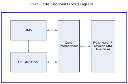
I'm studying Altera PCIe solution, and the Qsys design flow should suit for fresh man like me. I looked several examples, and found that all of them don't open interface to user logic, as attached image diagram shows.
Link Copied
9 Replies
- Mark as New
- Bookmark
- Subscribe
- Mute
- Subscribe to RSS Feed
- Permalink
- Report Inappropriate Content
Hi Jerry,
of course you can also use the PCIe solutions like in your blockdiagramm. If you want to use the Avalon MM Master or Slave interface outside of Qsys you have to export it to outside of qsys. An other solution is that you create some Qsys component and simply connect it.- Mark as New
- Bookmark
- Subscribe
- Mute
- Subscribe to RSS Feed
- Permalink
- Report Inappropriate Content
--- Quote Start --- Hi Jerry, of course you can also use the PCIe solutions like in your blockdiagramm. If you want to use the Avalon MM Master or Slave interface outside of Qsys you have to export it to outside of qsys. An other solution is that you create some Qsys component and simply connect it. --- Quote End --- Hi fberndl, Thanks for you reply! You mean i can export the on-chip memory outside the Qsys? Then my question is how to control the accessing to that on-chip memory? Since host(computer) and user logic may both want to access it. It seems i need to modify it to a dual-port ram, am i right?
- Mark as New
- Bookmark
- Subscribe
- Mute
- Subscribe to RSS Feed
- Permalink
- Report Inappropriate Content
Yeah you are right, if the host computer want to access the on chip memory and your user logic too you need an dual ported on chip memory. (look into my attachment) . But i think when you read some qsys tutorial or going trough an example this should be clear. look into Cyclone V Hard IP for PCI Express User Guide for example, this explains I think the usage for pcie cores.
- Mark as New
- Bookmark
- Subscribe
- Mute
- Subscribe to RSS Feed
- Permalink
- Report Inappropriate Content
--- Quote Start --- Yeah you are right, if the host computer want to access the on chip memory and your user logic too you need an dual ported on chip memory. (look into my attachment) . But i think when you read some qsys tutorial or going trough an example this should be clear. look into Cyclone V Hard IP for PCI Express User Guide for example, this explains I think the usage for pcie cores. --- Quote End --- Hi fberndl, I have several questions need you help. Maybe, they are very basic questions, but they are very important for me. 1. On the fpga logic side, how computer knows when user logic is ready for sending data to computer? On the other hand, how user logic knows when computer write data to FPGA? Can these different direction operations conflict each other? 2. As your example shows, when computer write some data into dual-ram, then user logic how to know that data is ready to be read by it(user logic)? The same question for computer is how it knows the data in dual-port ram is ready when user logic put some data into the ram?
- Mark as New
- Bookmark
- Subscribe
- Mute
- Subscribe to RSS Feed
- Permalink
- Report Inappropriate Content
Hi Jerry,
regarding synchronization. You can use the RX bars for HOST --> FPGA transfers . When you want to synchronize this transfer to your fpga logic you need a register in your fpga logic (DMA) for synchonization you can use the mSGDMA which can be found in the Altera Wiki, also some pcie designs. Which PCIe Designs did you looked into? For FPGA to Host transfers you write trough the Txs (Avalon MM Slave) interface to the system memory. You can assign an interrupt to the host. For this you need the mSGDMA with the respective registers. Just use one of the example designs from Altera or from the Altera Wiki. So the synchronization happens inside the dma and with interrupts!- Mark as New
- Bookmark
- Subscribe
- Mute
- Subscribe to RSS Feed
- Permalink
- Report Inappropriate Content
--- Quote Start --- Hi Jerry, regarding synchronization. You can use the RX bars for HOST --> FPGA transfers . When you want to synchronize this transfer to your fpga logic you need a register in your fpga logic (DMA) for synchonization you can use the mSGDMA which can be found in the Altera Wiki, also some pcie designs. Which PCIe Designs did you looked into? For FPGA to Host transfers you write trough the Txs (Avalon MM Slave) interface to the system memory. You can assign an interrupt to the host. For this you need the mSGDMA with the respective registers. Just use one of the example designs from Altera or from the Altera Wiki. So the synchronization happens inside the dma and with interrupts! --- Quote End --- Hello fberndl, Thanks for you kindly repley! I think i have downloaded that examples you pointed above. I will select one and look into deeply firstly. I remember something about those examples, they all looks something same as block diagram in my first post. Those examples only structure the host write data and read from ram(on-chip or external ddr-ram) inside Qsys. However, in real system the user logic need receive data from host and send user logic's data to host, both need thru Qsys. So my question and difficult is that i don't know how to modify those example design to fit my requirements. BTW, we are using Stratix IV GX devices. You last time recommend me reading pcie user guide of Cycone V, and i found something different between previous one. V serials have a new IP (pcie_avmm_dma), it seems DMA is embedded with pcie core. i attached the user guide. Anyway, thank you very much, more talks with you, more understand about pcie for me.
- Mark as New
- Bookmark
- Subscribe
- Mute
- Subscribe to RSS Feed
- Permalink
- Report Inappropriate Content
Hi Jerry,
you receive data trough the RxM_BAR interface when you look at page 17 in ug_pcie_avmm_dma . RX --> PCIe BARs. 1. Just go trough some user guide and examples and try to understand how the PCIe IP cores interfaces work and understand what the examples do. The user guide helps a lot. 2. Then you have to align your user design to these existing IP cores. (When you work in a company draw an blockdiagramm first..its always good)- Mark as New
- Bookmark
- Subscribe
- Mute
- Subscribe to RSS Feed
- Permalink
- Report Inappropriate Content
--- Quote Start --- Hi Jerry, you receive data trough the RxM_BAR interface when you look at page 17 in ug_pcie_avmm_dma . RX --> PCIe BARs. 1. Just go trough some user guide and examples and try to understand how the PCIe IP cores interfaces work and understand what the examples do. The user guide helps a lot. 2. Then you have to align your user design to these existing IP cores. (When you work in a company draw an blockdiagramm first..its always good) --- Quote End --- Thanks a lot! I will look into user guide and example firstly!
- Mark as New
- Bookmark
- Subscribe
- Mute
- Subscribe to RSS Feed
- Permalink
- Report Inappropriate Content
hi Jerry,
After reading the thread, I think I meet the same problem too. Now I want to transfer some datas from personal computer to the DDR4 on board via PCIe, while I don't know how to solve it. could you give me some advices? if you are Chinese, I wish I could add QQ buddy with you, and my account is 1092981053. wait for your kindly repley. thank you.
Reply
Topic Options
- Subscribe to RSS Feed
- Mark Topic as New
- Mark Topic as Read
- Float this Topic for Current User
- Bookmark
- Subscribe
- Printer Friendly Page