- Mark as New
- Bookmark
- Subscribe
- Mute
- Subscribe to RSS Feed
- Permalink
- Report Inappropriate Content
Hi Everyone,
I'm having a problem with Board Update Portal using the CycloneIVGX 4cgx150 Dev Kit. We are unable to Load a User Software image which is stored on the CFI device on our User Hardware Image using the Board Update Portal. My User Hardware design (Qsys Design) doesn't have an Flash Controller, so does that mean that my Base and End Address When I use elf2flash is the base and end Address of the Memory that I do use (Which is on chip-memory)? Should the Base and End address of the elf2flash be the actual User Software Area of the Memory device (0x01F2.0000 - 0x03FD.FFFF)? I am unable to find exactly where the elf .flash image is stored and why its stored there? If the Base Address is the flash components base address in the Qsys design how does the .flash 'know' where to move in the User Software Address range in the Flash Device? and If the Base Address is the Flash Device User Software Address (0x01F2.0000) why doesn't the elf2flash utility work? Ref: ug_civgx_fpga_dev_kit.pdf Alternative Nios II Boot Methods AN458.pdfLink Copied
4 Replies
- Mark as New
- Bookmark
- Subscribe
- Mute
- Subscribe to RSS Feed
- Permalink
- Report Inappropriate Content
I'm having the same issue as JayB. My design is for the Arria V starter board and included a NIOS that runs from on-chip memory and no flash memory. My on-chip memory is at address 0x0 and the cpu's reset vector is configured to point at 0x0. I've executed the following commands :
sof2flash --input=../../output_files/top.sof --output=top_hw.flash --offset=0x01640000 --pfl --optionbit=0x00018000 --programmingmode=FPP elf2flash --base=0x0000000 --end=0x07FFFFFF --reset=0x05280000 --input=ursa-nios.elf --output=ursa-nios_sw.flash The hardware boots but the NIOS never boots. JayB did you ever resolve this? Any insight would be greatly appreciated, Brian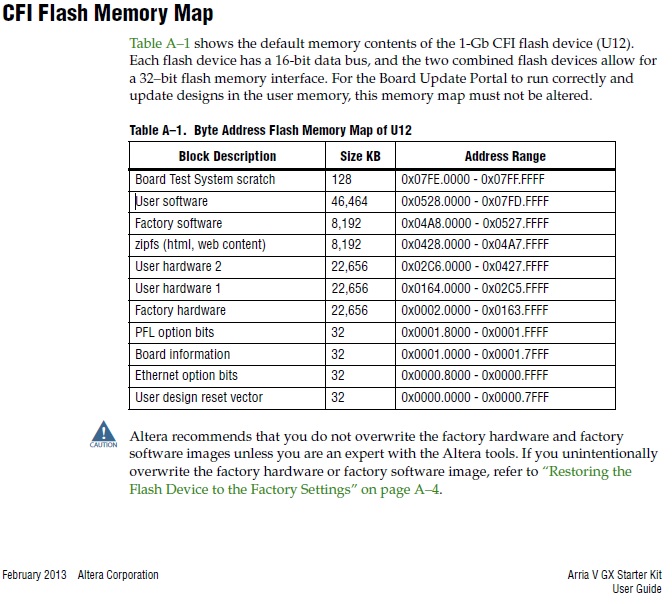
- Mark as New
- Bookmark
- Subscribe
- Mute
- Subscribe to RSS Feed
- Permalink
- Report Inappropriate Content
--- Quote Start --- My on-chip memory is at address 0x0 and the cpu's reset vector is configured to point at 0x0. .... The hardware boots but the NIOS never boots. --- Quote End --- Where is the Nios firmware actually stored? If it is supposed to be in user software section of CFI flash, cpu reset vector must be 0x05280000, not 0.
- Mark as New
- Bookmark
- Subscribe
- Mute
- Subscribe to RSS Feed
- Permalink
- Report Inappropriate Content
I will try it again after changing the reset vector. The elf2flash does output one warning and the it about the reset vectors not matching.
I'm a bit confused on where the firmware(NIOS code) is loaded. This dev board has a MAX V device that is attached to the FPGA and the flash and manages loading the FPGA. In the previous post I included an image of the CFI flash map. My intent is to load my hardware code into the "User Hardware 1" block and then to load my software into the "User Software" block. Then at power up, the Max V configures the FPGA based on a dip switch setting. Only one part of this process is working for me. It seems that the "User Hardware 1" is loaded at power up but I can't say what has happened with the "User Software". I can only say that the NIOS processor is not running. I'm not sure if the base of 0x0 is correct of if it should have been at another location.- Mark as New
- Bookmark
- Subscribe
- Mute
- Subscribe to RSS Feed
- Permalink
- Report Inappropriate Content
Usually the boot sequence is the following one:
- fpga configures from the factory hardware image - the nios system defined inside the factory hw boots the factory software - the factory software tests the dip switches (or whatever you use to select user application) and load the user configuration from the proper flash address. Before this phase usually the factory sw also starts a watchdog timer which pulls back fpga into factory configuration if anything goes wrong. - after the user configuration becomes active, it boots the user software image, loading it from the flash. The flash address is defined inside the nios system and must mutch the one where the sw image is actually stored. - the sw bootloader takes care of transferring flash image data to the required memory devices (onchip ram, sdram, ...) - if user sw is running properly, it clears the watchdog periodically (or disables it).
Reply
Topic Options
- Subscribe to RSS Feed
- Mark Topic as New
- Mark Topic as Read
- Float this Topic for Current User
- Bookmark
- Subscribe
- Printer Friendly Page