- Mark as New
- Bookmark
- Subscribe
- Mute
- Subscribe to RSS Feed
- Permalink
- Report Inappropriate Content
Hi,
I’m a student and I started my first FPGA project a few weeks ago. I want to create a “Bootloader” which programs my external flash memory via JTAG. At that point I program my flash memory via Boundary-Scan. But it takes too much time. Therefore I want to speed up the flash programming. I decided to create a Nios system with the embedded Peripherals IP. The “Bootloader” should be downloaded to the FPGA to configure it. Then the “Bootloader” should receive the flash content (program) via JTAG and write it to the flash memory. Could you please guide me through my project at points I don’t get further. Yet, I have less experience with FPGA’s but I’ll do my best. I have a Cyclone III FPGA Starter Kit for testing. First I want the “Bootloader” to run on the testing hardware. Afterwards, the “Bootloader” should run on another hardware. The major difference among the two hardware is the flash memory. I want to use Qsys to build the hardware. I think about following components to use: NIOS II/e : I don’t think I need a cache memory -> simplest processor JTAG UART : Should connect the host pc with the FPGA via JTAG to send programming data to flash On-chip (RAM) : 20K on-chip RAM for data and instructions of the NIOS II; data width: 32 Sysid : as a protection CFI-FLASH : Connection to the external flash memory Avalon-MM Tristate-Bridge: Connection to the external flash memory Is anything missing or should I use other components? I attached a screenshot which shows all connections of my system. Thank you for your help. Best regards.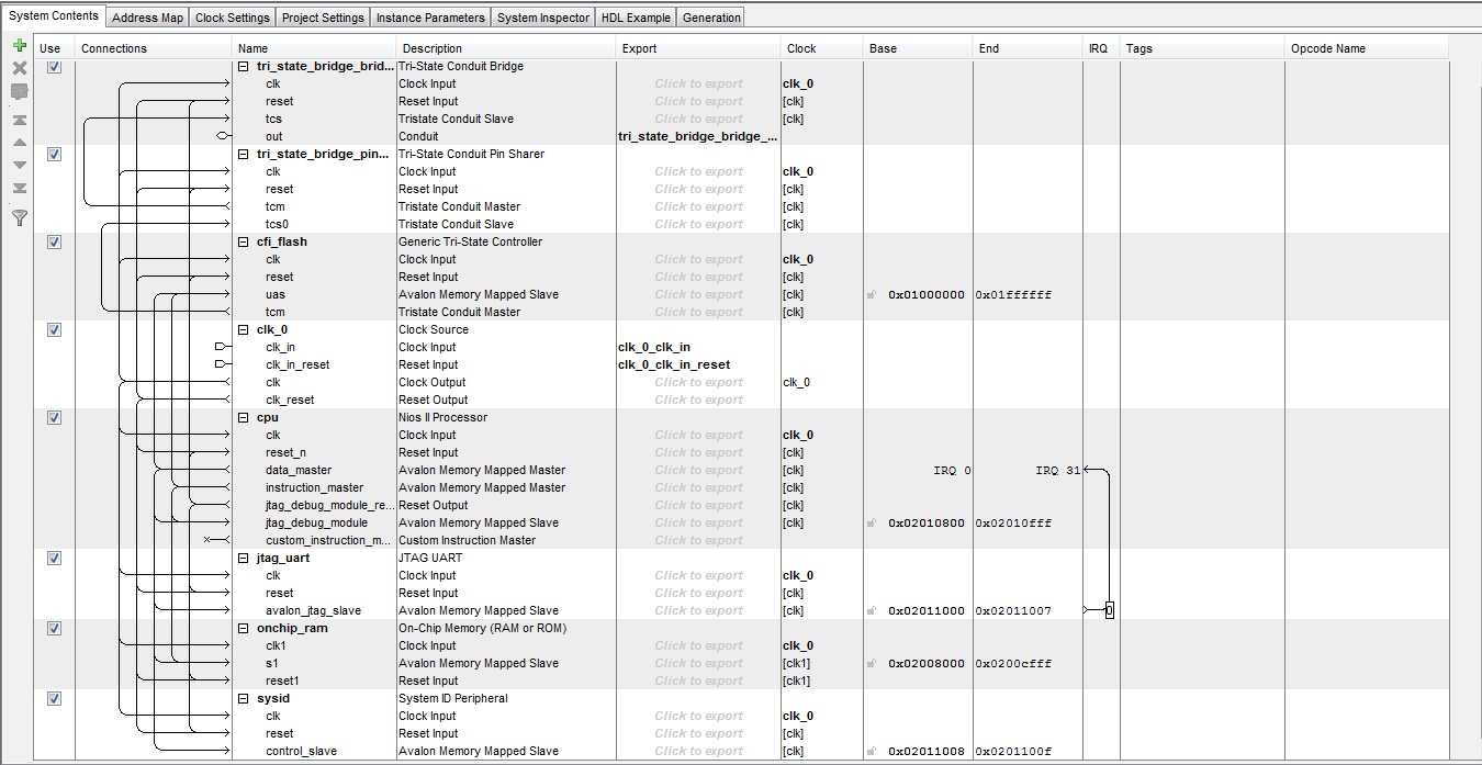
Link Copied
- Mark as New
- Bookmark
- Subscribe
- Mute
- Subscribe to RSS Feed
- Permalink
- Report Inappropriate Content
No this should be all you need.
An alternative to the Nios method could be to use an JTAG to Avalon bridge and connect it to the flash controller. Then you could use System Console on the PC to directly access the flash memory using master read/write commands.- Mark as New
- Bookmark
- Subscribe
- Mute
- Subscribe to RSS Feed
- Permalink
- Report Inappropriate Content
If you've built a design containing a Nios II processor and a flash controller (as it seems you have) then the nios2-flash-programmer executable supplied with Quartus can be used to program a hex file into your flash
- Mark as New
- Bookmark
- Subscribe
- Mute
- Subscribe to RSS Feed
- Permalink
- Report Inappropriate Content
Thanks for your response Daixiwen.
Although I’m very interested in your solution I want first to do it in the described way. Thus I will come back to your solution. But now I didn’t know exactly how to go on. I did the following steps: 1. Connect all components in Qsys as you can see in screenshot I attached 2. Generate this system (no warnings, no errors) 3. Instantiate this system in a .bdf to my Quartus project 4. Connect input-/outputs-pins to the block diagram 5. Add .qip to the project 6. Assign the pins in pin planner 7. Compile my project Is something missing or is it the right way to go on? Then I wanted to use the Flash Programmer from Nios II SBT for Eclipse to write data to flash memory. Therefore I downloaded my project to the FPGA first. After that I started the Flash Programmer and used the .sopcinfo from Qsys. Finally I add my .sof to files for flash conversion and clicked Start. I get the following error message: Error: Error code: 3 for command: $SOPC_KIT_NIOS2/bin/sof2flash --input="C:/Users/gger/Desktop/Quartus_Übungsprojekte/Quartus II/LED_Ansteuerung/LED.sof" --output="C:/Users/gger/Desktop/Bootloader_Files/Projekt_E3/flash/LED_flash_extern.flash" --offset=0x0 Do you have any idea what’s wrong?- Mark as New
- Bookmark
- Subscribe
- Mute
- Subscribe to RSS Feed
- Permalink
- Report Inappropriate Content
No I have no idea what an error code 3 is.... I would try to put the sof file in a folder that doesn't have non-ascii chatacters first... maybe the sof2flash binary doesn't like that 'Ü' character in the file path.
- Mark as New
- Bookmark
- Subscribe
- Mute
- Subscribe to RSS Feed
- Permalink
- Report Inappropriate Content
Thanls for your advice. But now I get another error message:
Info: No CFI table found at address 0x01000000 Info: Leaving target processor paused Error: Error code: 8 for command: $SOPC_KIT_NIOS2/bin/nios2-flash-programmer "C:/Users/gger/Desktop/Bootloader_Files/Projekt_E6/flash/LaufLi_cfi_flash.flash" --base=0x1000000 --sidp=0x2003008 --id=0x0 --timestamp=1342092177 --device=1 --instance=0 '--cable=USB-Blaster on localhost [USB-0]' --program Have you ever use the flash programmer? Did you recognize any mistakes in my actions? In addition to that I get 4 critical warnings: Critical Warning (332168): The following clock transfers have no clock uncertainty assignment. For more accurate results, apply clock uncertainty assignments or use the derive_clock_uncertainty command. Critical Warning (332169): From altera_reserved_tck (Rise) to altera_reserved_tck (Rise) (setup and hold) Critical Warning (332169): From altera_reserved_tck (Rise) to altera_reserved_tck (Fall) (setup and hold) Critical Warning (332169): From altera_reserved_tck (Fall) to altera_reserved_tck (Fall) (setup and hold) Do you know sth. about that? I don't know where to look.- Mark as New
- Bookmark
- Subscribe
- Mute
- Subscribe to RSS Feed
- Permalink
- Report Inappropriate Content
I haven't really used CFI flash chips... But the programmer seems to be looking at the correct place.
Did you create an .sdc file with timing constraints for TimeQuest? You should at least declare your clock inputs so that it can get the internal timing right. Then you'll probably need to constrain the CFI interface too. (and use the derive_clock_uncertainty to get rid of the critical warnings, but don't think those are related to your problem)- Mark as New
- Bookmark
- Subscribe
- Mute
- Subscribe to RSS Feed
- Permalink
- Report Inappropriate Content
hi......
if i understand you have a project with soc system running....... you need to write a .sof and .elf in your cfi_flash .....ok??? to write you need to convert the .sof and .elf in .flash files at nios2 command shell and in your project directory you need to do sof2flash --input=(your.sof) --output=(name.flash) --offset=(initial offset) --verbose your.sof = your project name.flash = the file generated initial offset = this is the offset of the flash memmory ...this is a data sheet parameter , i use 0x10000 at my flash and write your.flash nios2-flash-programmer --base=(your flash base addres) your.flash --verbose this write the .flash to convert the .elf elf2flash --after=(your.flash) --input=(your.elf) --output=(nios.flash) --boot=bootLoader_cfi.srec the bootloader file is at your quartus directory -> /altera/11/IP/ALTERA/NIOS2_IP/ALTERA_NIOS2/bootloader_cfi.srec remember to set up your RESET VECTOR in qsys write at nios2 command shel is very fast... cheers Franz- Mark as New
- Bookmark
- Subscribe
- Mute
- Subscribe to RSS Feed
- Permalink
- Report Inappropriate Content
Hello Franz,
first of all I'm sorry for the following "stupid" questions :oops:. My intention is to bridge the JTAG interface of the FPGA with the CFI interface of the flash memory. To cut a long story short, I want to create a PFL with a sopc system (in Qsys). Thus I want to write configuration data (.sof) to the flash memory. Every power-on the FPGA should configure from flash memory. But why do I need a .elf? For booting? Your solution sounds quite simple. Could you please explain it more detailed, because I didn't get everything. I would appreciate if you can explain it step by step. I even don't know, how to start the command shell?! I have just one more question. First I have to build a sopc system, generate it and instantiate it (e.g. with a .bdf) in my quartus project. Then I assign all pins, set all Dual-Purpose Pins to regular I/O and set configuration to Passive Serial (to get no "can't place multiple pins assigned to pin location...errors during compilation). Next, I compile my project and donwload the .sof to the FPGA. Now I'm able to program my flash memory with the command shell. Is that all right? Or did I misunderstand sth.?- Mark as New
- Bookmark
- Subscribe
- Mute
- Subscribe to RSS Feed
- Permalink
- Report Inappropriate Content
ok dude....
do you want program your external flash ... and use the fpga to do that??? or you want start the fpga with the program in you flash?? you dont need a paralel flash loader... you need to do a sopc with your system :cpu, jtag , tristate bridge, clock, cfi flash , clk_ref.... generate , instantiate, assign, etc.... and compile...... donwload the .sof goes to altera/nios2eds/nios2 command shell at your start menu (windows) and convert the file you want program to .flash and write the flash using nios2-flash-programmer....... i think that ..... explain better what you want to write to the flash...... cheers Franz- Mark as New
- Bookmark
- Subscribe
- Mute
- Subscribe to RSS Feed
- Permalink
- Report Inappropriate Content
You're right Franz. First I want to access/program my external flash (read and write operations) and use the fpga to do that. Thus I want to do a sopc.
Because I don't have much experience with sopc and Quartus, I would bid you to guide me through my first project. I think about making the major steps and then asking you if I forget sth. Consequently I would start a new project from the beginning. I think about the components you see in the screenshot I attached. Do I need the onchip_ram or should I delete it? Is the jtag_uart ok or is there a better component for jtag interface? Where should I set the reset vector memory and the exception vector memory? I think about the onchip_ram.s1 or the cfi_flash.s1! I'm very thankful for your help. Best Regards.
- Mark as New
- Bookmark
- Subscribe
- Mute
- Subscribe to RSS Feed
- Permalink
- Report Inappropriate Content
ok dude....
you need a onchip_ram....... is where your cpu will do the boot.... reset vector is where your FPGA program will start..... reset vector will set to your flash memory exception vector will set to your onchip ram .......is where your cpu boot the nios software jtag uart ok! good luck Franz- Mark as New
- Bookmark
- Subscribe
- Mute
- Subscribe to RSS Feed
- Permalink
- Report Inappropriate Content
OK. I set the reset vector to cfi_flash.s1 and the exception vector to onchip_ram.s1. The addresses will be automatically set by "Assign Base Address". Consequently I don't change them.
Then I generate this system. In Quartus project I open a new .bdf, instantiate the block diagramm of my system and connect the Inputs/Outputs (see in screenshot). In addition to that I add the .qip. After that I assign the pins as described in the reference manual (Cyclone 3 Starter Kit). When compiling the design I get "Can't place multiple pins assign to pin location H_3 error. Thus I go to Assignments -> Device -> Device and Pin Options -> Configuration site and select Passive Serial as Configuration Scheme. At the Dual-Purpose Pins site I set every pin to Use as regular I/O. Now I'm able to compile my project. Did I miss any step so far? Thanks again for your guidance.
- Mark as New
- Bookmark
- Subscribe
- Mute
- Subscribe to RSS Feed
- Permalink
- Report Inappropriate Content
After all these steps I downloaded the .sof to the fpga. Then I started the flash programmer from Nios II Eclipse (the flash programmer dialog box appears).
I did following steps: 1. File-> New -> Get flash Programmer details from SOPC Information file 2. Browse to right .sopcinfo and select it 3. I checked the values in Connections -> System ID Properties 4. At Files for flash conversion I add my .sof 5. Start the Flash Programmer But this doesn't work. I get the following error: Info: Info: ******************************************************************* Info: Info: Running Quartus II 32-bit Convert_programming_file Info: Info: Command: quartus_cpf --no_banner --convert C:/Users/gger/Desktop/BootloaderTest/Lauflicht/LaufLi.sof C:/Users/gger/Desktop/Bootloader_Files/Projekt_altera/flash/LaufLi_cfi_flash.rbf Info: Info: Quartus II 32-bit Convert_programming_file was successful. 0 errors, 0 warnings Info: Info: Peak virtual memory: 144 megabytes Info: Info: Processing ended: Wed Jul 18 09:34:31 2012 Info: Info: Elapsed time: 00:00:00 Info: Info: Total CPU time (on all processors): 00:00:00 Info: Using cable "USB-Blaster [USB-0]", device 1, instance 0x00 Info: Resetting and pausing target processor: OK Info: Reading System ID at address 0x02011008: verified Info: No CFI table found at address 0x01000000 Info: Leaving target processor paused Error: Error code: 8 for command: $SOPC_KIT_NIOS2/bin/nios2-flash-programmer "C:/Users/gger/Desktop/Bootloader_Files/Projekt_altera/flash/LaufLi_cfi_flash.flash" --base=0x1000000 --sidp=0x2011008 --id=0x0 --timestamp=1342588439 --device=1 --instance=0 '--cable=USB-Blaster on localhost [USB-0]' --program Do you ever got this error message? Do you know the reason for this error? Best regards.- Mark as New
- Bookmark
- Subscribe
- Mute
- Subscribe to RSS Feed
- Permalink
- Report Inappropriate Content
Ok lets do that.....
dont use the flash programmer at nios 22 eclipse..... go to start /programs /altera /nios2 EDS / nios2 legacy/ nios2 command shell and open the nios terminal and : sof2flash --input=(your.sof) --output=(output.flash) --offset=(initial offset) --verbose your.sof = your project output.flash = the file generated initial offset = this is the offset of the flash memmory ...this is a data sheet parameter , i use 0x10000 at my flash and write your.flash nios2-flash-programmer --base=(your flash base addres) output.flash --verbose do this and report Franz- Mark as New
- Bookmark
- Subscribe
- Mute
- Subscribe to RSS Feed
- Permalink
- Report Inappropriate Content
Ok, I will try the command shell option.
I write the commands you told me. But there is an error: "Input file, not found, or is not a valid SOF file"(see in screenshot). I guess the .sof is in a wrong directory. So could you please tell me in which directory the .sof belongs to? At the moment I have the following directory structure: desktop/Bootloader_Files/Projekt_altera -> there are all files (.qsys, .bsf, .qpf, ...) stored There are five more folders: .qsys_edit, Bootloader_Altera_E1, db, flash, incremental_db, script The .sof I want to write to flash is stored in another directory path: desktop/BootloaderTest/Lauflicht When I get this error message I copied the .sof from this directory path and paste it to desktop/Bootloader_Files/Projekt_altera, but still the same error. Where is the mistake in my actions? The offset value should be taken from datasheet, shouldn't it? I'm using 0x10, but the value isn't very important. It is just the offset within the flash where FPGA configuration is to be programmed, isn't it? Thus I can choose a arbitrary address. I start at the lowest programming region (as seen in screenshot). Sorry for getting on your nevres :). Best regards.- Mark as New
- Bookmark
- Subscribe
- Mute
- Subscribe to RSS Feed
- Permalink
- Report Inappropriate Content
ok ...good
looking at the print screen seens to me path error...... you copied the .sof to specify directory ....at the command shell you need to enter in this directory......type ls and check the files in directory.... and than type the command sof2flash my flash not use the first address (0x0 to 0x10000 datasheet)... and my offset need to check 0x10000.... good luck- Mark as New
- Bookmark
- Subscribe
- Mute
- Subscribe to RSS Feed
- Permalink
- Report Inappropriate Content
Ok, I did it as you told me.
First I changed the directory and now the conversion works fine and I get my .flash... ...but there is still the "No CFi table found at address 0x01000000" error. Thus I checked my base address in Qsys, but it's right. Do you ever get this error message? Do you got an idea how to eliminate it? Best regards.- Mark as New
- Bookmark
- Subscribe
- Mute
- Subscribe to RSS Feed
- Permalink
- Report Inappropriate Content
ok ...please verify the base address at .ptf file
download the .sof in your board before write try erase the flash ...... nios2-flash-programmer --base=(base) --erase-all what the cfi_flash do you use? rgs- Mark as New
- Bookmark
- Subscribe
- Mute
- Subscribe to RSS Feed
- Permalink
- Report Inappropriate Content
ok...I've done the erase command after downloading the .sof in my board...but still the same error and the same command shell window message.
Also I verified the base address in .qsys because I have no .ptf. I think this depends on which tool (Qsys or SOPC) you use...but it should be right. I'm using the Altera Cyclone III FPGA Starter Kit...on it a Intel 128P30 (8M x 16) parallel flash. The CFI Core uses default settings for this flash, so parameters concerning the flash should be allright. Could this error depend on pin assignment? Maybe we also should take a look at that. Do you ever work with a Dev-Board from Altera? I think my flash should be a 16-bit memory. Thus the Addr[0] is floating. It' s so annoying! What flash do you normally use? Best regards.- Subscribe to RSS Feed
- Mark Topic as New
- Mark Topic as Read
- Float this Topic for Current User
- Bookmark
- Subscribe
- Printer Friendly Page