- Mark as New
- Bookmark
- Subscribe
- Mute
- Subscribe to RSS Feed
- Permalink
- Report Inappropriate Content
Hi,
I am looking for a reference example, ideally for the DE0-Nano SoC (but any CycloneV SoC based example will do), that would allow me to test the following configuration:
a NIOS2 implemented in the FPGA, writing to a predefined area of the HPS's DDR3 memory.
I have plenty of examples implementing DMA controllers, but none of them quite correspond to this very simple setup. I do not need a DMA engine, I would like to dedicate the NIOS to reading data from input interfaces (UARTs) and writing them to the DDR3. I do not even need optimal performance, so going through the FPGA2Host bridge and not directly to the DDR3 controller will do just fine.
When I try to connect the NIOS2 directly to the f2h bridge of the HPS, QSys complains about the address range of the NIOS not being compatible with the 32 bit range of the f2h bridge. I understand this is because the NIOS can only handle 31 bits ?
Any pointers on how to do this very simple setup would be much appreciated (as you can tell, I am a beginner...)
Thanks
Link Copied
- Mark as New
- Bookmark
- Subscribe
- Mute
- Subscribe to RSS Feed
- Permalink
- Report Inappropriate Content
I will find a reference design for this application, but please first make sure you are using the NIOS as a master not slave.
- Mark as New
- Bookmark
- Subscribe
- Mute
- Subscribe to RSS Feed
- Permalink
- Report Inappropriate Content
Hi,
Yes, I am using NIOS as a master. I figured out a few things:
- first, that since I want to access both the HPS memory through the bridge, AND internal devices in the FPGA, I need to add an Address Span Expander, otherwise the whole 32 bit address space of the NIOS is mapped to the 32 bit space of the HPS memory, and there is no address left to access FPGA peripherals.
- So I added such an Address Span Expander, and I am mapping 16MB of the HPS memory, at HPS offset 0x32000000
But there is something I do not understand in Qsys behavior:
- when I initially connect the "expander master" port of the expander to the f2h bridge, everything seems to be fine:

- but if I do "Assign Base Addresses", then I get an error about NIOS not supporting address space above 32 bits: and I just noticed that this is because the addresses of all other peripherals have been recomputed and are now above 0xffffffff

Why does adding the expander and recomputing base addresses result in the remapped address being over the 32 bit address range ?
I am still interested in a simple reference example corresponding to this scenario, anyway.
Thank you,
- Mark as New
- Bookmark
- Subscribe
- Mute
- Subscribe to RSS Feed
- Permalink
- Report Inappropriate Content
Hi,
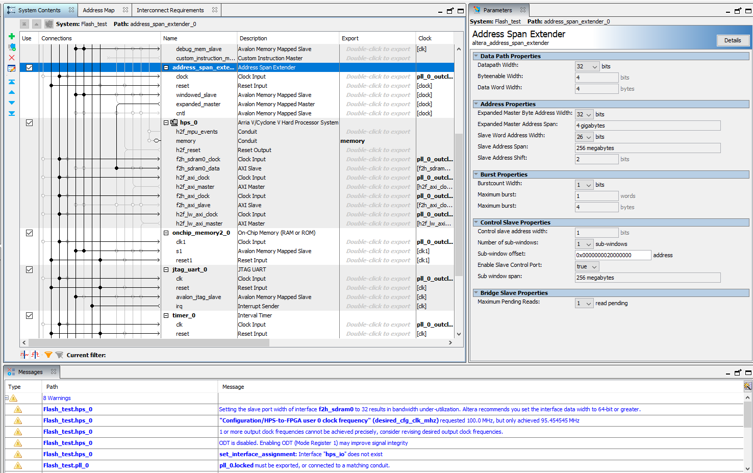
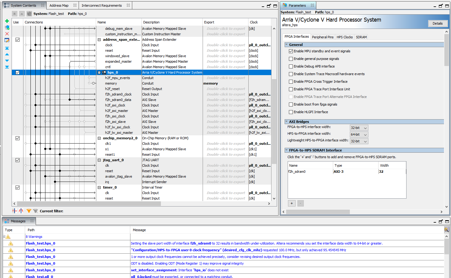
You have some errors in your connections, first, to access the DDR3 you must connect the span extender to F2H_sdram_data. I've tried to connect the system you need with no errors as show in the image below.
Also you can see the address span extender setting and the HPS setting
I will attach a design example tested already for the DE10_Nano (CV)
Regards,
- Mark as New
- Bookmark
- Subscribe
- Mute
- Subscribe to RSS Feed
- Permalink
- Report Inappropriate Content
- Mark as New
- Bookmark
- Subscribe
- Mute
- Subscribe to RSS Feed
- Permalink
- Report Inappropriate Content
- Mark as New
- Bookmark
- Subscribe
- Mute
- Subscribe to RSS Feed
- Permalink
- Report Inappropriate Content
- Mark as New
- Bookmark
- Subscribe
- Mute
- Subscribe to RSS Feed
- Permalink
- Report Inappropriate Content
Thanks a lot for the feedback and example, I fixed my design accordingly and things are working fine now.
- Subscribe to RSS Feed
- Mark Topic as New
- Mark Topic as Read
- Float this Topic for Current User
- Bookmark
- Subscribe
- Printer Friendly Page