- Mark as New
- Bookmark
- Subscribe
- Mute
- Subscribe to RSS Feed
- Permalink
- Report Inappropriate Content
Hi,
Please help me to clarify the relationship among these terms... 1. Suppose I want to move a batch of data from SDRAM to the registers or BRAMs on a custom module using Avalon MM fabric. Currently I know I've got roughly two design options depending on whether or not using Nios. Please let me know whether my understanding is correct or not, in addition, what's the pros and cons of the two options. 1) Use Nios: So Nios works as Avalon master, both external memory controller and my custom module have Avalon slave interface. These three components are connected in qsys. Then a C program in the Nios will do the data transaction using IOWR/IORD macros. In this case the data is read from SDRAM to Nios (either on-chip memory or external memory attached to Nios) before being written from Nios to custom module. 2) Without Nios: I'm not sure about this but this time my custom module is wrapped by Avalon MM master interface and is connected directly to the Avalon slave interface that wrap the external memory controller. Because there's no place for software, I need to construct RTL code to control signals from Avalon master interface (Basically a DMA of my own?). 2. What is the benefits of using DMA controller? In one of the tutorials "Using PCI express on DE4 boards", it says the data can be transferred between PCIe IP core and on-chip memory either directly or through DMA controller. If data transfer can be performed using Avalon MM bus directly then why do ppl use DMA controller? Please help me to understand the concept behind this, a simple example will be great! Please correct me if there's any mistake in the above description. ThanksLink Copied
7 Replies
- Mark as New
- Bookmark
- Subscribe
- Mute
- Subscribe to RSS Feed
- Permalink
- Report Inappropriate Content
Probably the easiest way to think about it is in terms of performance vs. resource utilization. Any of them will work.
Software is the slowest but uses the least resources, assuming you had the processor available already. DMA is faster than a processor and software, uses more resources, and you still usually need the processor to control it. The DMA can be shared across multiple components. An embedded Avalon-MM Master which performs it's own (bursting) transfers will be as fast as the DMA (or faster), but the FPGA resources are tied up in your component, and your component is a fair bit more complicated.- Mark as New
- Bookmark
- Subscribe
- Mute
- Subscribe to RSS Feed
- Permalink
- Report Inappropriate Content
--- Quote Start --- Probably the easiest way to think about it is in terms of performance vs. resource utilization. Any of them will work. Software is the slowest but uses the least resources, assuming you had the processor available already. DMA is faster than a processor and software, uses more resources, and you still usually need the processor to control it. The DMA can be shared across multiple components. An embedded Avalon-MM Master which performs it's own (bursting) transfers will be as fast as the DMA (or faster), but the FPGA resources are tied up in your component, and your component is a fair bit more complicated. --- Quote End --- Thanks Ted, Then if both DMA and Avalon MM Master can do the same job with close performance, why do we use both of them at the same time? I've seen a lot qsys design where DMA controller is added as a component and is connected with other components through Avalon MM bus. Does the combination offer other benefits? Thanks
- Mark as New
- Bookmark
- Subscribe
- Mute
- Subscribe to RSS Feed
- Permalink
- Report Inappropriate Content
--- Quote Start --- Then if both DMA and Avalon MM Master can do the same job with close performance, why do we use both of them at the same time? --- Quote End --- You might use them within the same system, but I don't think you would use them together at the same time. Post a link of a system structure which you are not sure about.
- Mark as New
- Bookmark
- Subscribe
- Mute
- Subscribe to RSS Feed
- Permalink
- Report Inappropriate Content
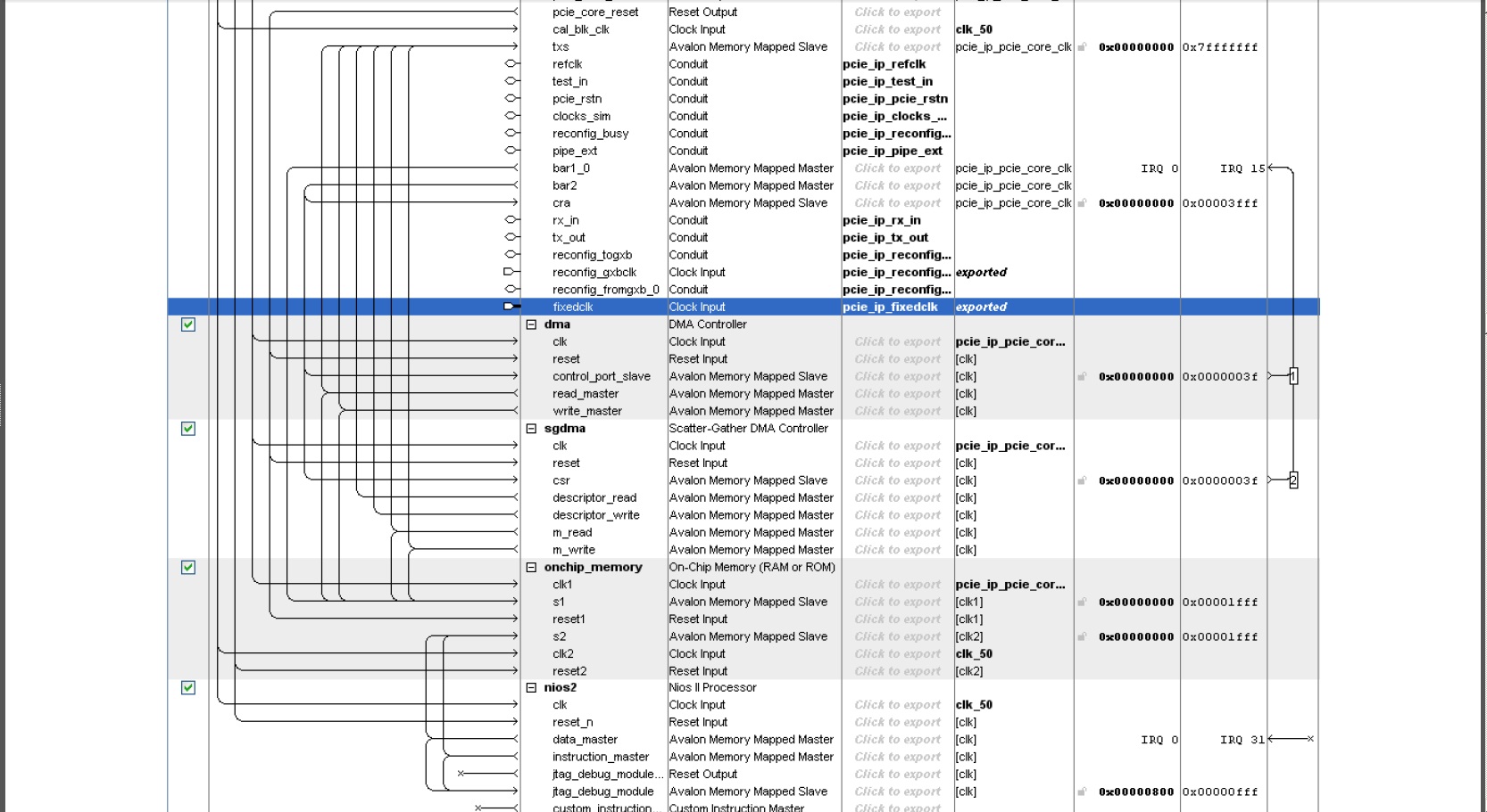
--- Quote Start --- You might use them within the same system, but I don't think you would use them together at the same time. Post a link of a system structure which you are not sure about. --- Quote End --- Ted, Please take a look at this screen shot, this is the qsys system constructed in the Altera tutorial "Using PCIe on DE4 boards". In the tutorial it says the PCIe IP core can be connected with the on-chip memory directly or through DMA/SGDMA. I guess the "direct connection" here means using Avalon-MM master/slave interface without DMA. However in the screen shot, in the case where a DMA is used, the components are still connected through Avalon-MM interface. This is what I mean by saying "Both DMA and Avalon-MM Master are used together at the same time" in the above post. https://www.alteraforum.com/forum/attachment.php?attachmentid=7263
- Mark as New
- Bookmark
- Subscribe
- Mute
- Subscribe to RSS Feed
- Permalink
- Report Inappropriate Content
PCIe is kind of a bad example to work from for this topic, because there are multiple subsystems (everything within the FPGA vs. everything on the other side of the PCIe pins; NIOS software and DMA controllers vs. (let's call it a PC) CPU and DMA controllers). All of those entities can read/write the "onchip_memory" component.
Why you would want to use one method vs. another depends on the specific task you are using that hardware design to perform. Kind of a typical use case would be having the FPGA transform or otherwise process some piece of data which originally is sitting inside the host CPU memory. You need to copy the data into the FPGA onchip_memory, command the operation to execute, and then retrieve the result. Getting back to why all the different methods, depends upon performance: - you can tie up the host CPU / DMA controllers and perform all of the memory transfers via the BAR1_0 Avalon-MM Master port. This is "entry level" complexity and frowned upon for more demanding applications. You typically would rather leave the host CPU and DMA free for other tasks, if possible. - you can have the host CPU command the Qsys "dma" DMA controller to process the memory transfers. The data would be transferred via the "txs" port shown in your diagram, and the FPGA would become the master of the data transfer in the PC. This arrangement is "better" than the previous one, since the host CPU is not tied up during the memory transfers, and simply has to control the "dma" peripheral. Finally, the most complicated / highest performance arrangement would be for the external CPU to command the NIOS software to autonomously manage the entire task. The NIOS would possibly then setup a number of descriptors for the SGDMA to continuously stream inputs / outputs to the host CPU memory. The control activity on the PC would maybe consists of issuing a "go" / "stop" command to the NIOS and maybe fielding interrupt notifications that the operations are completed. Anyway, there is possibly an infinite number of arrangements / applications that you can think up. But getting back to my original reply, it all boils down to performance / resources you want to dedicate to the task. This reference design you are looking at is fairly flexible, and allows for a single FPGA compilation to be used for an extended period of time while learning the software development ins and outs of PCIe systems. You can start with x86 peek/poke to the onchip memory, buffer transfers, etc. and then end with mailbox IPC to the NIOS with otherwise autonomous DMA between memories.- Mark as New
- Bookmark
- Subscribe
- Mute
- Subscribe to RSS Feed
- Permalink
- Report Inappropriate Content
Thanks a lot Ted for the profound explanation. I have a better understanding of this topic now!
- Mark as New
- Bookmark
- Subscribe
- Mute
- Subscribe to RSS Feed
- Permalink
- Report Inappropriate Content
Hi Ted,
I have created the Qsys design with Nios II processor connected to TXS port of PCIe hard ip to access the x86(host) processor DDR3 memory. I want to know after the driver allocate a memory in the host processor, how x86(host) processor writes the address of the memory to the address translation table? Please let me know if you required some more information. Thanks in advance.
Reply
Topic Options
- Subscribe to RSS Feed
- Mark Topic as New
- Mark Topic as Read
- Float this Topic for Current User
- Bookmark
- Subscribe
- Printer Friendly Page