- Mark as New
- Bookmark
- Subscribe
- Mute
- Subscribe to RSS Feed
- Permalink
- Report Inappropriate Content
I'm debugging a DDR2 SO-DIMM design that doesn't work (the example top design seemingly doesn't do anything). I enabled the debug interface per the EMI handbook (debug section) and ran the Debug GUI. The stage 'Read resynchronisation phase calibration - reset' fails with result code 0xa2177307.
Any idea where to start looking for errors? Would it make sense to lower the speed of the DDR2 interface (currently 200 MHz on an Arria II GX)? Any other tips? The only possible relevant warning is the following from analysis & synthesis: Warning: PLL "HPC1_example_top:inst1|HPC1:HPC1_inst|HPC1_controller_phy:HPC1_controller_phy_inst|HPC1_phy:HPC1_phy_inst|HPC1_phy_alt_mem_phy:HPC1_phy_alt_mem_phy_inst|HPC1_phy_alt_mem_phy_clk_reset:clk|HPC1_phy_alt_mem_phy_pll:half_rate.pll|altpll:altpll_component|altpll_u9p3:auto_generated|pll1" has parameters clk2_multiply_by and clk2_divide_by specified but port CLK[2] is not connected Is this normal? The .doom file is attached.Link Copied
- Mark as New
- Bookmark
- Subscribe
- Mute
- Subscribe to RSS Feed
- Permalink
- Report Inappropriate Content
I have today worked some more on this problem. It turns out that the exact same error occurs when the SO-DIMM module is removed from the socket. Interestingly enough, all the previous initialization reports as okay by the Debug GUI - seems odd.
I have also obtained more signaltap II signals at the point of failure. The attached JPG shows all signals recommended to be added to the signaltap trace (EMI Vol 4, section III - 'Debugging Hardware'). Not much can be gleaned from this information except that the s_rrp_reset state exited after 2 ticks and the FSM ended up in the s_non_operational (expected since the calibration failed). I will reverse engineer the details from the VHDL sources...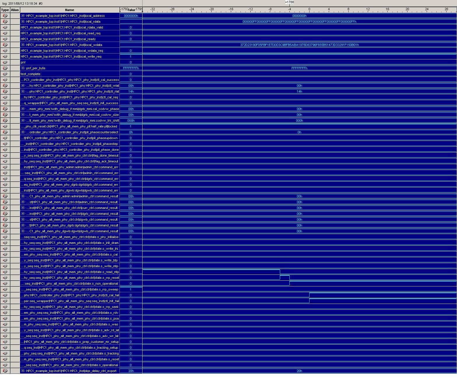
- Mark as New
- Bookmark
- Subscribe
- Mute
- Subscribe to RSS Feed
- Permalink
- Report Inappropriate Content
I have also attached the signaltap data file of all signals in my HPCII controller instance. The trace triggered on the first signal (ctl_init_fail). Can anyone spot where the error lies?
So far, by tracing back in the order the signals are asserted right before the trigger, this leads up to the error (older assertions listed first): HPC1_example_top:inst1|HPC1:HPC1_inst|HPC1_controller_phy:HPC1_controller_phy_inst|HPC1_phy:HPC1_phy_inst|HPC1_phy_alt_mem_phy:HPC1_phy_alt_mem_phy_inst|HPC1_phy_alt_mem_phy_seq_wrapper:seq_wrapper|HPC1_phy_alt_mem_phy_seq:seq_inst|HPC1_phy_alt_mem_phy_ctrl:ctrl|mtp_err HPC1_example_top:inst1|HPC1:HPC1_inst|HPC1_controller_phy:HPC1_controller_phy_inst|HPC1_phy:HPC1_phy_inst|HPC1_phy_alt_mem_phy:HPC1_phy_alt_mem_phy_inst|HPC1_phy_alt_mem_phy_seq_wrapper:seq_wrapper|HPC1_phy_alt_mem_phy_seq:seq_inst|HPC1_phy_alt_mem_phy_ctrl:ctrl|ctrl_mmi.ctrl_current_stage.cmd_rrp_reset HPC1_example_top:inst1|HPC1:HPC1_inst|HPC1_controller_phy:HPC1_controller_phy_inst|HPC1_phy:HPC1_phy_inst|HPC1_phy_alt_mem_phy:HPC1_phy_alt_mem_phy_inst|HPC1_phy_alt_mem_phy_seq_wrapper:seq_wrapper|HPC1_phy_alt_mem_phy_seq:seq_inst|HPC1_phy_alt_mem_phy_ctrl:ctrl|dis_state HPC1_example_top:inst1|HPC1:HPC1_inst|HPC1_controller_phy:HPC1_controller_phy_inst|HPC1_phy:HPC1_phy_inst|HPC1_phy_alt_mem_phy:HPC1_phy_alt_mem_phy_inst|HPC1_phy_alt_mem_phy_seq_wrapper:seq_wrapper|HPC1_phy_alt_mem_phy_seq:seq_inst|HPC1_phy_alt_mem_phy_ctrl:ctrl|last_state.s_non_operational (HPC1_example_top:inst1|HPC1:HPC1_inst|HPC1_controller_phy:HPC1_controller_phy_inst|HPC1_phy:HPC1_phy_inst|HPC1_phy_alt_mem_phy:HPC1_phy_alt_mem_phy_inst|HPC1_phy_alt_mem_phy_seq_wrapper:seq_wrapper|HPC1_phy_alt_mem_phy_seq:seq_inst|HPC1_phy_alt_mem_phy_ctrl:ctrl|ctrl_mmi.ctrl_err_code = 17h) HPC1_example_top:inst1|HPC1:HPC1_inst|HPC1_controller_phy:HPC1_controller_phy_inst|HPC1_phy:HPC1_phy_inst|HPC1_phy_alt_mem_phy:HPC1_phy_alt_mem_phy_inst|HPC1_phy_alt_mem_phy_seq_wrapper:seq_wrapper|HPC1_phy_alt_mem_phy_seq:seq_inst|HPC1_phy_alt_mem_phy_ctrl:ctrl|ctrl_mmi.ctrl_calibration_fail HPC1_example_top:inst1|HPC1:HPC1_inst|HPC1_controller_phy:HPC1_controller_phy_inst|HPC1_phy:HPC1_phy_inst|HPC1_phy_alt_mem_phy:HPC1_phy_alt_mem_phy_inst|HPC1_phy_alt_mem_phy_seq_wrapper:seq_wrapper|HPC1_phy_alt_mem_phy_seq:seq_inst|HPC1_phy_alt_mem_phy_ctrl:ctrl|ctrl_mmi.master_state_r.s_non_operational HPC1_example_top:inst1|HPC1:HPC1_inst|HPC1_controller_phy:HPC1_controller_phy_inst|HPC1_phy:HPC1_phy_inst|ctl_cal_fail It looks like the source seems to be 'mtp_err' which would mean that the problem lies in the PREVIOUS calibration state (MTP Pattern Writes) although reported as successful in the Debug GUI (see earlier posts). Thanks.- Mark as New
- Bookmark
- Subscribe
- Mute
- Subscribe to RSS Feed
- Permalink
- Report Inappropriate Content
Does the example project generated by the IP work?
- Mark as New
- Bookmark
- Subscribe
- Mute
- Subscribe to RSS Feed
- Permalink
- Report Inappropriate Content
--- Quote Start --- Does the example project generated by the IP work? --- Quote End --- No, this is the project i'm running. The project generated by the IP must however be modified to run in a real FPGA. I have essentially created a new top-level block that connects to the clock pin and DDR2 SO-DIMM pins. Inside, the test HPCII DDRs 'driver' and controller are used as-is.
- Mark as New
- Bookmark
- Subscribe
- Mute
- Subscribe to RSS Feed
- Permalink
- Report Inappropriate Content
I don't have any RUP/RDN pins connected to my FPGA. Apparently, this is needed for the DDR2 interface to function properly? Is there any workaround to salvage the board or will I have to respin the board?
- Mark as New
- Bookmark
- Subscribe
- Mute
- Subscribe to RSS Feed
- Permalink
- Report Inappropriate Content
Signal Integrity is still important at 200MHz. You could check your interface and see if the eye looks ok. The fact that the cal is failing at an early stage could be explained by bad SI.
- Mark as New
- Bookmark
- Subscribe
- Mute
- Subscribe to RSS Feed
- Permalink
- Report Inappropriate Content
I tried to lower the interface speed to 125 MHz but without luck. Are the RUP and the RDN resistors required? Will the interface fail like described if the HPCII calibration block is not used? I designed my SODIMM interface per the Arria II GX devkit but missed the RUP and RDN pins.
- Mark as New
- Bookmark
- Subscribe
- Mute
- Subscribe to RSS Feed
- Permalink
- Report Inappropriate Content
Rup/Rdn is required, the OCT is calibrated of them. Cal block is required too.
- Mark as New
- Bookmark
- Subscribe
- Mute
- Subscribe to RSS Feed
- Permalink
- Report Inappropriate Content
--- Quote Start --- Rup/Rdn is required, the OCT is calibrated of them. Cal block is required too. --- Quote End --- thank you. will the lack of cal block and resistors result in the error I'm seeing? Is there any way to make my ddr2 interface work without the resistors or will I need to respin the board?
- Mark as New
- Bookmark
- Subscribe
- Mute
- Subscribe to RSS Feed
- Permalink
- Report Inappropriate Content
You'd need to check your SI. I'd recommend both scoping it and simulating it.
- Mark as New
- Bookmark
- Subscribe
- Mute
- Subscribe to RSS Feed
- Permalink
- Report Inappropriate Content
It turns out that the calibration block is only needed if calibrated termination is used in the design. The HPCII MegaWizard by default created a tcl script that set the DDR2 I/O signals to 'calibrated serial 50 ohm'. After changing them to 'serial 50 ohm' (non-calibrated) the design started working. I'm now running the test bench at 150 MHz with signaltap II and the Debug GUI and everything works okay.
I will next bring up the DDR2 clock speed to see how far I can go with uncalibrated serial termination. question: What is the difference between CALIBRATED and non-calibrated termination? Is it merely the value of the termination resistor that is tuned automatically for ideal signal integrity over PVT? My DDR2 interface is rather slow (150 MHz to 200 MHz will do) so I could likely "get away" with non-calibrated termination (although the RUP/RDN resistors are easy to add in for the next board respin - just in case).- Subscribe to RSS Feed
- Mark Topic as New
- Mark Topic as Read
- Float this Topic for Current User
- Bookmark
- Subscribe
- Printer Friendly Page