- Mark as New
- Bookmark
- Subscribe
- Mute
- Subscribe to RSS Feed
- Permalink
- Report Inappropriate Content
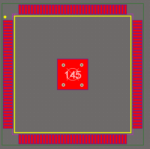
I use MAX10 10M08SAE144 for my design. When I design the footprint for this chip, I read this from pin information document: " The E144-pin package has an exposed ground pad at the bottom of the package. The exposed ground pad is used for electrical connectivity and not for thermal purposes. You must connect the exposed ground pad to the ground plane of the PCB". In order to save routing path, can I drill some vias on this pad which connect to the ground plane, instead of connect this pad to other ground pins through wires?
- Mark as New
- Bookmark
- Subscribe
- Mute
- Subscribe to RSS Feed
- Permalink
- Report Inappropriate Content
Absolutely you want to connect the ground pad directly to the ground plane. Don't use long traces to wire it to the other ground pins. They should connect direct to the ground plane as well with a local via per pin. Ditto for VCC pins that connect to a VCC plane (if present).
As to whether you can have VIAs directly within the EPAD it depends on the capability of your PCB vendor and assembly house. Some allow VIA-in-PAD, others may not want you to do that, and instead have the VIAs just outside the EPAD connected by short traces.
Link Copied
- Mark as New
- Bookmark
- Subscribe
- Mute
- Subscribe to RSS Feed
- Permalink
- Report Inappropriate Content
Absolutely you want to connect the ground pad directly to the ground plane. Don't use long traces to wire it to the other ground pins. They should connect direct to the ground plane as well with a local via per pin. Ditto for VCC pins that connect to a VCC plane (if present).
As to whether you can have VIAs directly within the EPAD it depends on the capability of your PCB vendor and assembly house. Some allow VIA-in-PAD, others may not want you to do that, and instead have the VIAs just outside the EPAD connected by short traces.
- Subscribe to RSS Feed
- Mark Topic as New
- Mark Topic as Read
- Float this Topic for Current User
- Bookmark
- Subscribe
- Printer Friendly Page
