- Mark as New
- Bookmark
- Subscribe
- Mute
- Subscribe to RSS Feed
- Permalink
- Report Inappropriate Content
Any layout guide for EP4CE15M9I7N for DDR2 routing?
As it's very small pintch 0.5mm, and we need to consider impedance match, it's not easy to route the trace. Any layout guide line?
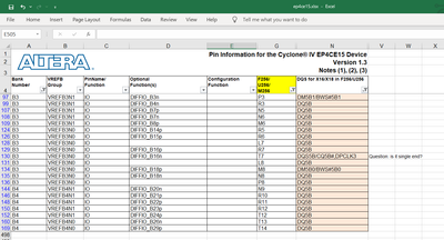
In the pinout file, it defines T3 of Bank3 as DQS.
1) Only this pin can be used as DQS?
2) DQS pin of DDR2 ram is differential, why it specified only one pin?
Link Copied
- Mark as New
- Bookmark
- Subscribe
- Mute
- Subscribe to RSS Feed
- Permalink
- Report Inappropriate Content
Hi XShen1,
Unfortunately, the layout for the EPACE15M9I7N is not available.
The PIN_T7 should be assigned as DQS pin location.
But if you find that the DQS is differential, you can let the Quartus to assign the other pin location during the Fitter compilation.
The DDR2 interface are differential or single ended.
Regards,
Adzim
- Mark as New
- Bookmark
- Subscribe
- Mute
- Subscribe to RSS Feed
- Permalink
- Report Inappropriate Content
I still see below problem.
1) If use single end, at least 2 DQS are needed for 16 bit DDR2. Why only pin T7 is assigned?
2) If use differential, another pin should R7 as pair of T7, but it's already assigned to DQ signal.
- Mark as New
- Bookmark
- Subscribe
- Mute
- Subscribe to RSS Feed
- Permalink
- Report Inappropriate Content
Hi XShen1,
I've referred to internal team and confirm that the device is only supported the single ended data strobe.
I hope that answer your question.
Regards,
Adzim
- Mark as New
- Bookmark
- Subscribe
- Mute
- Subscribe to RSS Feed
- Permalink
- Report Inappropriate Content
Thank you, you answered 50%. For 16 bit, there are 2 DQS even single end, but there is only 1 DQS pin assigned in pinout file, this is the other question.
- Mark as New
- Bookmark
- Subscribe
- Mute
- Subscribe to RSS Feed
- Permalink
- Report Inappropriate Content
Hi Xshen1,
When you're using the DQ X16 configuration, there should be only one DQS within that DQ Group.
Thanks,
Adzim
- Subscribe to RSS Feed
- Mark Topic as New
- Mark Topic as Read
- Float this Topic for Current User
- Bookmark
- Subscribe
- Printer Friendly Page
