- Mark as New
- Bookmark
- Subscribe
- Mute
- Subscribe to RSS Feed
- Permalink
- Report Inappropriate Content
Hi,
I have created simple schematic design [consists of 4-bit counter and Ibufout-diff [from IP catlog]. While compilation, it`s showing error. one more issue is, i have assigned only 4 pins[3..0], but in pin planner its taking extra pin count. I dont know why. Please look over my design and Pin planner diagram.Link Copied
6 Replies
- Mark as New
- Bookmark
- Subscribe
- Mute
- Subscribe to RSS Feed
- Permalink
- Report Inappropriate Content
Your pictures are way too small to see anything.
- Mark as New
- Bookmark
- Subscribe
- Mute
- Subscribe to RSS Feed
- Permalink
- Report Inappropriate Content
Hi,
Also if possible attach the project? or Save the message/error and attach. Best Regards, Anand Raj Shankar (This message was posted on behalf of Intel Corporation)- Mark as New
- Bookmark
- Subscribe
- Mute
- Subscribe to RSS Feed
- Permalink
- Report Inappropriate Content
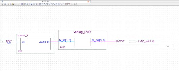
--- Quote Start --- Hi, Also if possible attach the project? or Save the message/error and attach. Best Regards, Anand Raj Shankar (This message was posted on behalf of Intel Corporation) --- Quote End --- I am unable to upload the project. So please check my attachment. In Schematic design, total output pins are 4. But in Pin planner output ports are missing only clk and reset pin is available
- Mark as New
- Bookmark
- Subscribe
- Mute
- Subscribe to RSS Feed
- Permalink
- Report Inappropriate Content
I don't see any output pins on your schematic design
- Mark as New
- Bookmark
- Subscribe
- Mute
- Subscribe to RSS Feed
- Permalink
- Report Inappropriate Content
--- Quote Start --- I don't see any output pins on your schematic design --- Quote End --- I am new to Altera Quartus. Doing LVDS testing from Altera Cyclone to Xilinx Board. Can anyone conform whether my block design is right or wrong. Design Flow sending input from 4-bit counter to single-ended input and differential output Alter buffer. Then passing differential output LVDS signal from Cyclone V board to Xilinx Custom Board. I tried lot but it is not working. So, anyone please guide me.
- Mark as New
- Bookmark
- Subscribe
- Mute
- Subscribe to RSS Feed
- Permalink
- Report Inappropriate Content
It looks fine now. Be sure to select the LVDS I/O type for your output pins in the pin planner.
Reply
Topic Options
- Subscribe to RSS Feed
- Mark Topic as New
- Mark Topic as Read
- Float this Topic for Current User
- Bookmark
- Subscribe
- Printer Friendly Page