- Mark as New
- Bookmark
- Subscribe
- Mute
- Subscribe to RSS Feed
- Permalink
- Report Inappropriate Content
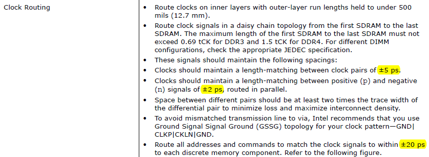
Some design guidelines in EMIF user guide use "ps" as unit, as you can see in the following screenshot.
But in the pcb design, I must check the route lines by mils or millimeter, how can I convert "ps" in the EMIF layout guidelines to "mil"?
Thanks, regards.
Link Copied
- Mark as New
- Bookmark
- Subscribe
- Mute
- Subscribe to RSS Feed
- Permalink
- Report Inappropriate Content
Well, all the physical devices care about is ps of timing delay for aligning signal edges.
When it comes to converting ps of delay to mils of trace length, it depends entirely on your PCB implementation.
Whether you are using stripline, microstrip, or embedded microstrip, and the dielectric material of your PCB all determine the Tpd or ps/mil delay factor for your PCB.
Most PCB layout tools have calculators that allow you to enter the stackup configuration and Er (dielectric constant) of your PCB material so they can compute Tpd.
Some PCB layout packages allow you to enter net length parameters in terms of 'ps' instead of 'mil' (or 'mm') but again you must configure the detailed stackup.
So if none of this makes any sense to you I suggest you find an SI (Signal Integrity) guy in your organization to help you.
- Mark as New
- Bookmark
- Subscribe
- Mute
- Subscribe to RSS Feed
- Permalink
- Report Inappropriate Content
Thanks.
Is Tpd the time delay which the signal propagate in 1 mil?
The unit of Tpd is ps/mil, is that correct?
Regards.
- Mark as New
- Bookmark
- Subscribe
- Mute
- Subscribe to RSS Feed
- Permalink
- Report Inappropriate Content
In my above answer I use Tpd to refer to the propagation delay factor for a given trace, and it would be specified in the units of ps/mil (or ps/in, or ps/cm, or some length/time unit).
So if you then need to do a, for example 100ps delay on a trace with a Tpd factor of 170ps/inch (a quite common PCB velocity factor) the trace would be ~590 mils in length.
Most PCB velocity factors (for standard epoxy fiberglass materials) in the range of 100-200ps/inch. More exotic dielectrics (like teflon, etc) can be quite different.
I find the Saturn PCB toolkit (free download at http://www.saturnpcb.com/pcb_toolkit/) to be quite helpful for examining PCB characteristics.
- Mark as New
- Bookmark
- Subscribe
- Mute
- Subscribe to RSS Feed
- Permalink
- Report Inappropriate Content
Thank you very much for your answer, that is really helpful.
- Mark as New
- Bookmark
- Subscribe
- Mute
- Subscribe to RSS Feed
- Permalink
- Report Inappropriate Content
Hello SYiwe,
The reason Intel recommended guideline in pico second (ps) is due to variety of substances used in PCB manufacturing process which might have different trace length which also mentioned by @ak6dn .
Good news for you! I found the older version of the EMIF handbook which apply the board guideline in mils. Refer to this link -->
https://pdfs.semanticscholar.org/7a14/f0cef20b74cb964d728e7c0feca89fd46333.pdf
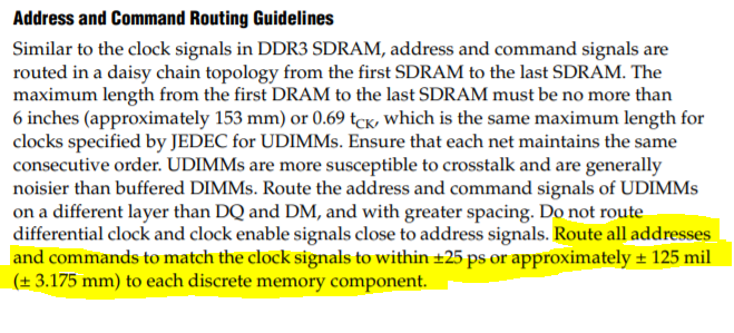
Routing for address and command routing, Intel recommendations is approximately ± 125 mil (± 3.175 mm) or within ±25ps to each discrete memory component. You may refer to “Layout Considerations For DIMMs and Leveled Components” on page 79 for more information about layout guidelines in above shared link. I also attached below screenshots on both clock , add/cmd routing to ease your viewing.
I summarize the formula ( based on our document) . This is similar as per shared by @ak6dn but I converted it based on our documentation.
125mil = 0.125inch
25ps/0.125inch = 200ps/inch
In short, you can use "200ps/inch" to calculate the delay/length based on your board.
Hope this helps.😊
And thanks @ak6dn for the very useful information 😊
Thanks
Regards,
Aida
- Mark as New
- Bookmark
- Subscribe
- Mute
- Subscribe to RSS Feed
- Permalink
- Report Inappropriate Content
Thanks.
I believe the problem is solved.
Regards.
- Subscribe to RSS Feed
- Mark Topic as New
- Mark Topic as Read
- Float this Topic for Current User
- Bookmark
- Subscribe
- Printer Friendly Page


