- Mark as New
- Bookmark
- Subscribe
- Mute
- Subscribe to RSS Feed
- Permalink
- Report Inappropriate Content
I'm using 10M08SAE144C8G with Quartus 18.1 Lite Edition.
I found this warning when I compile my project "
Warning (15055): PLL "PLL:inst_PLL|altpll:altpll_component|PLL_altpll:auto_generated|pll1" input clock inclk[0] is not fully compensated and may have reduced jitter performance because it is fed by a non-dedicated input
Info (15024): Input port INCLK[0] of node "PLL:inst_PLL|altpll:altpll_component|PLL_altpll:auto_generated|pll1" is driven by clk_ext~inputclkctrl which is OUTCLK output port of Clock control block type node clk_ext~inputclkctrl"
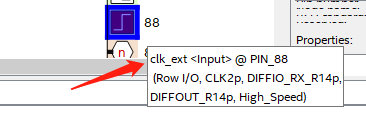
I assigned the dedicated clock input port to connect the input port of PLL, but I don't know why the CLKCTRL module is added?
Will this warning affect the clock quality in my design? If it does, how can I eliminate the CLKCTRL module on the clock path? Thank you.
This is the technology map viewer:
Link Copied
- Mark as New
- Bookmark
- Subscribe
- Mute
- Subscribe to RSS Feed
- Permalink
- Report Inappropriate Content
Hi,
When driving the PLL using the GCLK network, the input and output delays might not be fully compensated in the Quartus Prime software.
Try by giving timing constrains and PLL Compensation assignments using the Assignment Editor(Assignment Name->Global Signal CLKCNTRL location). Which will eliminate the warning.
Checked it using PLL In source-synchronous compensation mode, In zero-delay buffer mode
Let me know if this has helped resolve the issue you are facing or if you need any further assistance.
Regards
Anand
- Mark as New
- Bookmark
- Subscribe
- Mute
- Subscribe to RSS Feed
- Permalink
- Report Inappropriate Content
Thank you for your reply. I'd like to describe my scenario more clearly at first. The external clock is connected to the dedicated clock pin, then it is directly connected to the PLL in my code. The OUTPUT pin of the PLL is feed to the global clock network, so it is the PLL to drive the GCLK network.
My purpose is to remove CLKCTRL module instead of changing its location by using the assignment "Global Signal CLKCNTRL location". This is because there was no CLKCTRL module between the dedicated clock pin and PLL input pin when this project was running on Quartus 9.0 with Cyclone III. This CLKCTRL module appeared when the whole project was migrated to MAX10 chip with Quartus 18.1 Lite currently. Therefore, I would be appreciated if there is a solution that can eliminate the CLKCTRL in the clock path which makes the design the same as the original one.
- Mark as New
- Bookmark
- Subscribe
- Mute
- Subscribe to RSS Feed
- Permalink
- Report Inappropriate Content
Hi,
Can you share the project ?
So that I can replicate the scenario.
Regards
Anand
- Subscribe to RSS Feed
- Mark Topic as New
- Mark Topic as Read
- Float this Topic for Current User
- Bookmark
- Subscribe
- Printer Friendly Page

