- Mark as New
- Bookmark
- Subscribe
- Mute
- Subscribe to RSS Feed
- Permalink
- Report Inappropriate Content
Regarding the use of the Seriallite II protocol in hardware: The chip we use is the EP2AGX65DF29C6N of the Arria II GX series. When using quartus II to allocate the pins, it is not clear how the input and output of the Seriallite II IP core should be connected to the chip pins. Hereby ask for help, hoping to solve the problem.
Link Copied
- Mark as New
- Bookmark
- Subscribe
- Mute
- Subscribe to RSS Feed
- Permalink
- Report Inappropriate Content
Hi,
As I understand it, you have some inquiries related to the SLII IP. Sorry as I am not very clear with your specific inquiries related to connecting the SLII IP to the FPGA pins. To ensure we are on the same page, would you mind to further elaborate on the specific pin that you are referring to i.e. transceiver pins and etc.
For your information, you may also refer to the example testbench for further details on interconnecting the IPs. You may refer to the SLII IP user guide -> SLII IP Core Testbench section for further details.
Please let me know if there is any concern. Thank you.
- Mark as New
- Bookmark
- Subscribe
- Mute
- Subscribe to RSS Feed
- Permalink
- Report Inappropriate Content
Thank you for your reply.
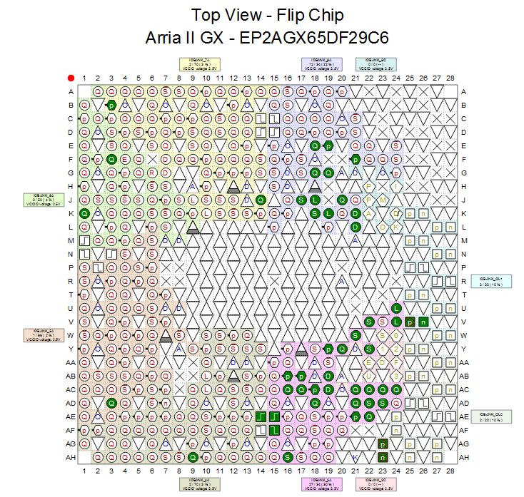
Regarding the pin connection, the specific problem is this: On the SLII IP, there are data input and output pins, such as rxin, txout, rxrdp_dat[], txrdp_dat[], etc., as well as some other signal pins (with bsf attached).
And on the FPGA chip we use (with pin diagram attached), there are ten banks, of which there are two GXB banks, divided into general purpose I/O, high-speed differential I/O, high-speed differential I/O with DPA, and we also want to use LVDS.
Therefore, we want to find out which bank or IO port these signals on the SLII IP should be connected to, and whether you have any other opinions and suggestions on the use of LVDS in this process.
Looking forward to your reply.
- Mark as New
- Bookmark
- Subscribe
- Mute
- Subscribe to RSS Feed
- Permalink
- Report Inappropriate Content
Hi,
Thanks for your update. For your information, the involved IOs seems to range across few types of IOs and it would be rather difficult for me to comment on which pin to use for a specific port.
Just wonder if you plan to port all the IOs of the SLII IP to the FPGA pins?
My recommendation would be for you to let the Fitter perform auto placement for your design if you do not have a specific placement location requirement for now. Generally Fitter will perform the placement for optimal performance provided if you have set the constraints ie SDC constraints upfront. If you encounter any issue along the way, then we could further work out from there.
I am more towards the SLII IP itself and in case you encounter any LVDS IO related problem during the auto-placement, we can further engage the LVDS team to further assist.
Please let me know if there is any concern. Thank you.
- Mark as New
- Bookmark
- Subscribe
- Mute
- Subscribe to RSS Feed
- Permalink
- Report Inappropriate Content
Thank you for your reply.
I have tried to let Fitter perform automatic placement for the design, and set the location according to the setting of the fitter location (pictured), but there is a problem when using LVDS: the I/O standard of the rxin signal can be set to LVDS, but the I/O standard of the txout signal cannot be set to LVDS, only 1.4-V PCML, 1.5-V PCML, 2.5V (default) can be set.
When I tried to connect the txout signal to other banks, the following error occurred:
Error (167081): I/O standard "LVDS" on I/O pin "txout1" is incompatible with the GXB channel's VCCH voltage setting "1.5V"
Error (169004): I/O pin txout1 with Termination logic option setting OCT 100 Ohms cannot be assigned to pin W10 - pin does not support logic option setting
So I want to ask, in the seriallite II IP core,
whether the rxin and txout signals can only be connected to the GXB bank?
Does the txout signal confirm that LVDS cannot be used?
What type of SFP transceiver can be used for 1.5-V PCML?
Another: The FPGA document I refer to is
https://www.intel.com/content/dam/www/programmable/us/en/pdfs/literature/dp/arria-ii-gx/ep2agx65.pdf
Looking forward to your reply.
- Mark as New
- Bookmark
- Subscribe
- Mute
- Subscribe to RSS Feed
- Permalink
- Report Inappropriate Content
Hi,
Thanks for your update. Please see my comments as following:
1. the I/O standard of the rxin signal can be set to LVDS, but the I/O standard of the txout signal cannot be set to LVDS, only 1.4-V PCML, 1.5-V PCML, 2.5V (default) can be set.
[CP] Yes, you are right. If you are using GXB, the TX only support 1.4-V PCML and 1.5-V PCML but no LVDS. You may refer to the device datasheet -> "Transceiver Specifications" for further details
2. whether the rxin and txout signals can only be connected to the GXB bank?
[CP] Yes, they can be connected to GXB bank only.
3. What type of SFP transceiver can be used for 1.5-V PCML?
[CP] It is recommended for you to cross check the transceiver specs in the device datasheet against the SFP modules that you plan to use to ensure they are compatible.
Please let me know if there is any concern. Thank you.
- Mark as New
- Bookmark
- Subscribe
- Mute
- Subscribe to RSS Feed
- Permalink
- Report Inappropriate Content
Thank you for your reply.
Regarding the 1.5V PCML level standard, I only found information about the CML level standard when searching for information. I was a little confused. What is the difference between these two? Is there any information about the PCML level standard?
In addition, I noticed that the main difference between CML and LVDS lies in the voltage swing and data transmission rate. Does SFP that can use LVDS also can use CML?
Finally, there is a question about voltage. SFP is powered by 3.3V. The level standard we use for data transmission on FPGA is 1.5V PCML. Is there any influence between these two voltages? My understanding is that these two are separate and powered by different power sources, so there is no need to consider 3.3V and 1.5V when connecting. Is this understanding correct?
Looking forward to your reply.
- Mark as New
- Bookmark
- Subscribe
- Mute
- Subscribe to RSS Feed
- Permalink
- Report Inappropriate Content
Hi,
Sorry as I might have overlooked this. Please allow me some time to look into your latest inquiries related to the PCML. Please ping me if you do not hear back from me by end of the week.
- Mark as New
- Bookmark
- Subscribe
- Mute
- Subscribe to RSS Feed
- Permalink
- Report Inappropriate Content
Hi,
Regaring the PCML, as I understand it, it is a standard defined in our transceiver. You may refer to the device datasheet -> "Transceiver Specification" for the specs supported by our transceiver when configured with PCML IO standard.
Regarding your inquiry CML and LVDS, you would need to cross check with the link partners' datasheet to ensure both sides are compatible. For our FPGA, you can check the device datasheet transceiver specification and then compare with 3rd party device's interface requirement/specs. All the transceiver specs need to be compatible.
Regarding your 3rd question on SFP, sorry as I am not familiar with you SFP module. Similar to the above, you would need to ensure the FPGA - SFP modules' interfaces are compatible by checking the interfaces' specs.
Please let me know if there is any concern. Thank you.
- Mark as New
- Bookmark
- Subscribe
- Mute
- Subscribe to RSS Feed
- Permalink
- Report Inappropriate Content
Hi,
As I understand it, it has been some time since I last heard from you. This thread will be transitioned to community support. If you have a new question, feel free to open a new thread to get the support from Intel experts. Otherwise, the community users will continue to help you on this thread. Thank you.
- Subscribe to RSS Feed
- Mark Topic as New
- Mark Topic as Read
- Float this Topic for Current User
- Bookmark
- Subscribe
- Printer Friendly Page