- Mark as New
- Bookmark
- Subscribe
- Mute
- Subscribe to RSS Feed
- Permalink
- Report Inappropriate Content
Hello everyone.
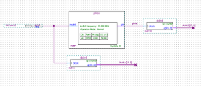
In my board i have 3V3 oscillator connect wints pin clk0 of my cyc3 fpga.
For example : Oscillator is 33mhz SG5032CAN here : https://fr.farnell.com/epson/x1g0044510006-sg5032can-33-mhz-tjga/oscillateur-spxo-sg5032can-33/dp/2442988RL?st=oscillateur%2033mhz
I want use it to generate multiple clocks
I try a simple counter divider and i try pll
I'm learning at some documentions, i see a doc with tff toggle or with a " inverter dff and not "
i need multiple clocks with different speeds in my design
After a lot of testing / compilation there are often functions that not operational. Is random !
Can you give me a solution?
Thanks in advance.
Regard.
Link Copied
- Mark as New
- Bookmark
- Subscribe
- Mute
- Subscribe to RSS Feed
- Permalink
- Report Inappropriate Content
There's no need to do this. Just enable a second PLL output and use it as a pass-through, matching the properties of the input clock.
- Mark as New
- Bookmark
- Subscribe
- Mute
- Subscribe to RSS Feed
- Permalink
- Report Inappropriate Content
Thank you Sstrell .
Please, can you give me a example shematic or where can i find an example ?
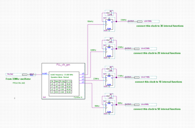
One source (4 or 8 mhz ) will be connected to around 40 or more receiving functions.
The other clocks will be connected to about 20 receiver functions.
- Mark as New
- Bookmark
- Subscribe
- Mute
- Subscribe to RSS Feed
- Permalink
- Report Inappropriate Content
I'm not sure I understand what you're saying. But what I'm saying is to go into the IP Parameter Editor for the PLL and enable additional clock outputs there. So you'd have the c0 like you have in the schematic but also a c1, which can be independently configured.
- Mark as New
- Bookmark
- Subscribe
- Mute
- Subscribe to RSS Feed
- Permalink
- Report Inappropriate Content
Thank you.
Apart from the clk0 leg of the FPGA , my design is in the FPGA .
I try this example, but it does not work .
I did not draw the functions that receive the clocks .
Are there functions "like buffers" in Quartus to multiply the same signals ?
Thanks again in advance .
Regard .
- Mark as New
- Bookmark
- Subscribe
- Mute
- Subscribe to RSS Feed
- Permalink
- Report Inappropriate Content
Why are you adding additional clock dividers on the outputs of the PLL? Just set the output clocks of the PLL to what you want in the parameter settings for the PLL and then connect those outputs to your logic.
When you say "it does not work", what does that mean? What happens? Errors?
- Mark as New
- Bookmark
- Subscribe
- Mute
- Subscribe to RSS Feed
- Permalink
- Report Inappropriate Content
Hello
Thank you for your reply.
Indeed, adding a frequency divider behind a clock signal does not seem normal to me.
Could you tell me how you would go about generating clock signals similar to the last electrical diagram I posted ?
Can we use directly the clock signals generated by the PLL to 50 receiver functions?
Does Quartus take into account the number of receiving functions?
Precisely I do not know if it need buffers?
Example Quartus message : Warning: Can't achieve minimum setup and hold requirement clk33 along 6649 path(s). See Report window for details .
Thank you in advance.
- Mark as New
- Bookmark
- Subscribe
- Mute
- Subscribe to RSS Feed
- Permalink
- Report Inappropriate Content
Again, just set up the PLL with the clocks you need and connect directly, no buffers needed. There is nothing else you need to do.
Without those dividers in the path, the compiler will most likely automatically put your clocks on the global clock routing channels, which are high fanout, low skew networks to help meet timing. You should have a .sdc file with timing constraints that defines these clocks as well.
- Mark as New
- Bookmark
- Subscribe
- Mute
- Subscribe to RSS Feed
- Permalink
- Report Inappropriate Content
Hello
Very thank for your replie(s)
I try it today.
Best regards .....
- Mark as New
- Bookmark
- Subscribe
- Mute
- Subscribe to RSS Feed
- Permalink
- Report Inappropriate Content
Hi,
May I know if you have any updates?
Thanks
Best regards,
KhaiY
- Mark as New
- Bookmark
- Subscribe
- Mute
- Subscribe to RSS Feed
- Permalink
- Report Inappropriate Content
Hello an thanks for following up on this discussion.
I use Quartus 9.0 in an old PC ant i try "classic timming analyser" and "Timequest timming analyser"
It's difficult to set up any clock node.
In my design i have 8 baseds clocks 33, 8, 4, ..... to 1 Mhz . Fmax are 33Mhz.
I have trouble to set up parameters for Quartus to take them into account .
After compiling , with classic timming i have this message :
Warning: Can't achieve minimum setup and hold requirement clk33 along 8752 path(s). See Report window for details .
I imagine this warning indicates that signals are not connected?
clk33 are pin input clock clk0, my FPGA are ep3c10c8n. I use ~80% of cell and combinations fuctional and ~2500 logic registers
When i use timequest timming analyser there is apparently no error , is this normal in your opinion ?
Thank in advance.
Regards.
- Mark as New
- Bookmark
- Subscribe
- Mute
- Subscribe to RSS Feed
- Permalink
- Report Inappropriate Content
>> I imagine this warning indicates that signals are not connected?
No, it probably means your "clocks" are not on global clock networks as @sstrell explained. The point of global and regional clocks is to provide a low-skew path to a large amount of logic.
>> When i use timequest timming analyser there is apparently no error , is this normal in your opinion ?
If you don't setup any constraints, you won't get any errors. Did you set the input clock frequency in your constraints. Also, you should put derive_pll_clocks in your .sdc file.I never understood why that was not the default, but without it the tools seem to assume the output clocks are the same frequency as the input clock.
Altera had some great free online training that would probably benefit you greatly. I think one was called something like "Becoming an FPGA Designer in 4 hours".
- Mark as New
- Bookmark
- Subscribe
- Mute
- Subscribe to RSS Feed
- Permalink
- Report Inappropriate Content
Hello and Thank you for your reply.
Also i try Advisor function and timming optimisation advisor fuction.
It tell some settings, whet this setting are aplied it increase compiling time and it reduce the number of warnings
Regards.
- Mark as New
- Bookmark
- Subscribe
- Mute
- Subscribe to RSS Feed
- Permalink
- Report Inappropriate Content
Hi,
May I know if you have any updates?
Thanks
Best regards,
KhaiY
- Mark as New
- Bookmark
- Subscribe
- Mute
- Subscribe to RSS Feed
- Permalink
- Report Inappropriate Content
Hi,
We do not receive any response from you to the previous question/reply/answer that I have provided. This thread will be transitioned to community support. If you have a new question, feel free to open a new thread to get the support from Intel experts. Otherwise, the community users will continue to help you on this thread. Thank you
Best regards,
KhaiY
- Mark as New
- Bookmark
- Subscribe
- Mute
- Subscribe to RSS Feed
- Permalink
- Report Inappropriate Content
Hello
Excuse my delay
I 'm learning Quartus documentation.
if you ask me I will keep you posted on my progress on this subject.
I managed with 2 CLKLOCK functions, a prioris it takes a PLL resource from my FPGA
Best regards
- Subscribe to RSS Feed
- Mark Topic as New
- Mark Topic as Read
- Float this Topic for Current User
- Bookmark
- Subscribe
- Printer Friendly Page

