- Mark as New
- Bookmark
- Subscribe
- Mute
- Subscribe to RSS Feed
- Permalink
- Report Inappropriate Content
Hi,
in a project I want to use MAX V (precisely: 5M40ZE64I5N) operating as a slave on SPI bus, so I've started to prepare a very simple module for communication over SPI bus. My device uses 5 lines: nrst - reset, negative logic, ncs - chip select, negative logic, sck - clock, mosi - input of data to MAX V, miso - output of data from MAX V. I have a strange problem with outputting data on the miso line. I'd appreciate any hint on what's the cause, please. I'm using Quartus II 64-Bit Version 15.0.0 Build 145 04/22/2015 SJ Web Edition. The code is attached. As you can see, the module gets ready for work once nrst is high and ncs gets low, then it should output data on the miso line, the data change on falling edge of clock sck. The data should be an sequence of alternating '1's and '0's, starting with a '1'. The input line mosi is ignored. Quartus shows the RTL diagram that I'd expect to see: https://alteraforum.com/forum/attachment.php?attachmentid=14156&stc=1 The simulator (gate level simulation in ModelSim AE) says it should work as assumed: https://alteraforum.com/forum/attachment.php?attachmentid=14157&stc=1 however the oscilloscope shows something different: https://alteraforum.com/forum/attachment.php?attachmentid=14158&stc=1 yellow - sck (2V/div) green - miso (2V/div) time scale 20us/div (so it's ca. 120kbit/s) The first bit is set correctly as '1', then the first falling edge triggers transition to '0', and the next falling edges are ignored. Why? Best regards, Adam- Tags:
- Clock
Link Copied
4 Replies
- Mark as New
- Bookmark
- Subscribe
- Mute
- Subscribe to RSS Feed
- Permalink
- Report Inappropriate Content
No particular reason in design, may be an unclean clock signal with ringing edge? I presume reset and ncs are driven correctly.
- Mark as New
- Bookmark
- Subscribe
- Mute
- Subscribe to RSS Feed
- Permalink
- Report Inappropriate Content
The clock is shown on the oscillogram in the first post, it looks good to me. I've measured slopes of the edges, the transitions occur in less than 100ns.
Yes, ncs and nrst are driven correctly - I've checked that. I've also tried to provide a create_clock constraint in SDC file, but that didn't help. However with different timings, the output could display also other values, but 10101010 only appeared incidentally. Is it possible that I get synthesized something else instead of the flip-flop? How to check that?- Mark as New
- Bookmark
- Subscribe
- Mute
- Subscribe to RSS Feed
- Permalink
- Report Inappropriate Content
I've had a look at the logic element used for toggling the output and I wonder if the drawing is accurate, i.e. the connections which are shown are to be taken seriously, or is it "just a drawing". The configured LE looks like this:
https://www.alteraforum.com/forum/attachment.php?attachmentid=14159 My question relates to the connections shown inside the "rectangle on the left", which, if I understand correctly, is the lookup table. If these connections represent anything physical, then DATAD input cannot reach the flipflop.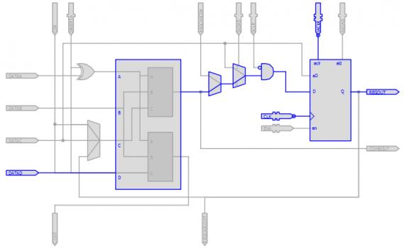
- Mark as New
- Bookmark
- Subscribe
- Mute
- Subscribe to RSS Feed
- Permalink
- Report Inappropriate Content
RTL and gate level schematics are just a logic visualization, if there's a fault I won't overrate it.
I think it's just a misleading display. Similarly the gate level schematic for MAX V misses the feedback signal inversion, but if you go to the resource property editor, it's finally shown. I'm not working with MAX II/V in any active design now and can't check the operation of this simple circuit in actual hardware. I remember that Quartus synthesis had some problems with classic CPLD like MAX3000, but MAX II/V uses essentially Cyclone alike FPGA logic elements and should be synthesized similarly. There's a certain chance of a bug related to MAX V in newer Quartus versions. I suggest to advance to useful SPI logic circuits and check if the problems stay. Timing constraints don't affect logic implementation in the first order.
Reply
Topic Options
- Subscribe to RSS Feed
- Mark Topic as New
- Mark Topic as Read
- Float this Topic for Current User
- Bookmark
- Subscribe
- Printer Friendly Page