- Mark as New
- Bookmark
- Subscribe
- Mute
- Subscribe to RSS Feed
- Permalink
- Report Inappropriate Content
Hello everyone,
I'm currently working on an FPGA design project and have encountered a problem that I hope to get some guidance on. The issue arises when trying to connect one of our intermediate outputs directly to the least significant bit of the ALTDDIO_IN IP's input data port. Specifically, the error message I receive is as follows:
Error (15871): Input port DATAIN of DDIO_IN primitive "ddio:uut|altddio_in:ALTDDIO_IN_component|ddio_in_2of:auto_generated|ddio_ina[0]" must come from an I/O IBUF or DELAY_CHAIN primitive.
Here’s a simplified version of the relevant part of my design:
Link Copied
- Mark as New
- Bookmark
- Subscribe
- Mute
- Subscribe to RSS Feed
- Permalink
- Report Inappropriate Content
Hello Sir,
I'm Adzim, application engineer will assist you in this case.
I require some information in the points below to debug this problem:-
- Which Quartus version that you're using?
- Which FPGA device that you're using?
- Can you provide the IP name as in Platform Designer/Quartus?
- Which compilation stage is failing?
Regards,
Adzim
Regards,
Adzim
- Mark as New
- Bookmark
- Subscribe
- Mute
- Subscribe to RSS Feed
- Permalink
- Report Inappropriate Content
Hi Adzim
Thanks for your response. Our actual production code is running on Quartous Prime 19.1 standard edition but this demo code is running on Quartous Prime 20.1 edition. In our Production device we are using cyclone V 5CEBA4U15C7 device. In our design we are using ALTDDIO_IN ip. Analysis and synthesis stage it is failing.
Thanks & regards,
Sameer
- Mark as New
- Bookmark
- Subscribe
- Mute
- Subscribe to RSS Feed
- Permalink
- Report Inappropriate Content
Hi Adzim,
Thanks for your response. Our actual production code is running on Quartous Prime 19.1 standard edition but this demo code is running on Quartous Prime 20.1 edition. In our Production device we are using cyclone V 5CEBA4U15C7 device. In our design we are using ALTDDIO_IN ip. Analysis and synthesis stage it is failing.
Thanks & regards,
Sameer
- Mark as New
- Bookmark
- Subscribe
- Mute
- Subscribe to RSS Feed
- Permalink
- Report Inappropriate Content
Hi,
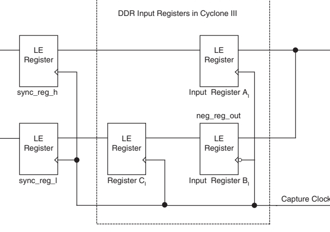
I think the error message is rather clear. DDIO_IN is expecting input from IO-pin but you are connecting it to a register. If actually need DDR register function in fpga fabric, you build it from registers.
- Mark as New
- Bookmark
- Subscribe
- Mute
- Subscribe to RSS Feed
- Permalink
- Report Inappropriate Content
Hi,
But if we want to double the data rate of an intermediate value, then how to use this IP in our design. We are debugging something. So we attach some intermediate value as input to DDIO_IN. Can you please suggest, how to double the data rate of intermediate registor value.
Thanks
- Mark as New
- Bookmark
- Subscribe
- Mute
- Subscribe to RSS Feed
- Permalink
- Report Inappropriate Content
DDIO_IN does not double a data rate. It splits a double data rate stream into two single data rate streams as shown in my previous post. Please explain in detail what you want to achieve.
- Mark as New
- Bookmark
- Subscribe
- Mute
- Subscribe to RSS Feed
- Permalink
- Report Inappropriate Content
Hi,
I am using DDIO_IN ip to get the input data both in positive and negative edge of clock. E.g., let my input signal = 7'b0000001. Then I want this input signal will appear as output for both positive and negative clock. Then I will combine this two data and make it as a 14 bit output data.
E.g.,
wire [13:0]data_output;
reg [6:0]data_input;
DDIO_IN(
);
In this way I want to double the data rate of input 7 bit to 14 bits data. That's what I want to perform,
- Mark as New
- Bookmark
- Subscribe
- Mute
- Subscribe to RSS Feed
- Permalink
- Report Inappropriate Content
As mentioned, DDIO IP is only for DDR data on I/O pins. I think you simply want to have separate clocked processes.
always @(posedge clk)
dataout_h <= ...
always @(negedge clk)
dataout_l <= ...
- Subscribe to RSS Feed
- Mark Topic as New
- Mark Topic as Read
- Float this Topic for Current User
- Bookmark
- Subscribe
- Printer Friendly Page